Analog Interfacing to Embedded
Microprocessors Real World DesignAnalog Interfacing to Embedded
MicroprocessorsReal World DesignStuart BallBoston Oxford Auckland Johannesburg Melbourne New Delhi
Newnes is an imprint of
Butterworth –Heinemann.
Copyright © 2001 by Butterworth–Heinemann
A
member of the Reed Elsevier group
All rights reserved.
No
part of this publication may be reproduced,
stored in a retrieval system, or transmitted in
any form or by any
means , electronic,
mechanical , photocopying, recording, or otherwise,
without the
prior written permission of the
publisher .
Recognizing the
importance of preserving what has been written, Butterworth–Heinemann
prints its
books on acid-free
paper whenever possible.
Library of Congress Cataloging-in-Publication Data
Ball, Stuart R., 1956 –
Analog interfacing to embedded microprocessors : real world design / Stuart Ball.
p.
cm.
ISBN 0-7506-7339-7 (pbk. : alk. paper)
1. Embedded computer systems—Design and construction.
2. Microprocessors.
I. Title.
TK7895.E42 .B33
2001
004.16—dc21
00-051961
British Library Cataloguing-in-Publication Data
A catalogue record for this book is
available from the British Library.
The publisher offers
special discounts on bulk orders of this book.
For information, please contact:
Manager of Special
Sales Butterworth-Heinemann
225 Wildwood Avenue
Woburn, MA 01801-2041
Tel: 781-904-2500
Fax: 781-904-2620
For information on all Newnes publications available, contact our World
Wide Web home page
at:
http://www.newnespress.co m
10 9 8 7 6 5 4 3 2 1
Printed in the United
States of America
ContentsPrefaceixIntroductionxi1System Design1 Dynamic Range1Calibration2Bandwidth5Processor Throughput6Avoiding Excess Speed 7 Other System Considerations8Sample Rate and Aliasing112 Digital -to-Analog Converters 13Analog-to-Digital Converters15 Types of ADCs17Sample and Hold 26Real Parts29Microprocessor Interfacing30 Serial Interfaces36Multichannel ADCs41 Internal Microcontroller ADCs41Codecs42Interrupt Rate43 Dual - Function Pins on Microcontrollers43Design Checklist45v
3 Sensors 47Temperature Sensors47Optical Sensors59CCDs72Magnetic Sensors82 Motion /Acceleration Sensors86 Strain Gauge904 Time- Based Measurements93Measuring Period versus Frequency 95Mixing97 Voltage -to-Frequency Converters99 Clock Resolution1025 Output Control Methods103 Open - Loop Control103 Negative Feedback and Control103Microprocessor-Based Systems104On-Off Control105 Proportional Control108PID Control110 Motor Control123Measuring and Analyzing Control Loops1306 Solenoids, Relays, and Other Analog Outputs137Solenoids137Heaters143Coolers148 Fans 149LEDs1517 Motors161 Stepper Motors161DC Motors180Brushless DC Motors184Tradeoffs between Motors198Motor Torque201vi
Contents8 EMI203 Ground Loops203ESD2089 High- Precision Applications213Input Offset Voltage215Input Resistance 216Frequency Characteristics 217Temperature Effects in Resistors218Voltage References219Temperature Effects in General221Noise and Grounding222 Supply -Based References22710 Standard Interfaces229IEEE 1451.22294-20 ma Current Loop231 Appendix A: Opamp Basics233 Four Opamp Configurations233General Opamp Design Equations237Reversing the Inputs238Comparators239Instrumentation Amplifiers243Appendix B: PWM245Why PWM?245Real Parts250 Audio Applications252Appendix C: Some Useful URLs255Glossary257Index261Contentsvii
PrefaceThere often
seems to be a
division between the analog and digital worlds.
Digital designers
usually do not like to delve into analog, and analog design-
ers
tend to
avoid the digital realm. The two groups often do not
even use the
same buzzwords.
Even though microprocessors have become increasingly faster and more
capable, the real world remains analog in
nature . The digital designers who
attempt to control or
measure the real world must somehow connect this
analog environment to their digital machines. There are books about analog
design and books about microprocessor design. This book attempts to get at
the problems encountered in
connecting the two together.
This book
came about because of a comment made by
someone about my
first book (
Embedded Microprocessor Systems: Real World Design): “it
needs more
analog interfacing information.” I
felt that
adding this
material to that book
would
cause the book to
lose focus .
However , the more I
thought about it,
the more I thought that a book aimed at interfacing the real world to micro-
processors
could prove valuable . This book is the
result . I
hope it proves
useful.
ix
IntroductionModern electronic systems are increasingly digital: digital microprocessors,
digital
logic , digital interfaces. Digital logic is
easier to design and
understand ,
and it is much more flexible
than the
equivalent analog circuitry would be.
As an example,
imagine trying to
implement any kind of sophisticated micro-
processor with analog parts. Digital electronics lets the PC on your desk
execute
different programs at different
times ,
perform complex calculations,
and communicate via the World Wide Web.
While the electronic world is
nearly all digital, the real world is not. The
temperature in your office is not just hot or
cold , but varies over a wide range.
You can use a thermometer to determine what the temperature is, but how
do you
convert the temperature to a digital
value for use in a microprocessor-
controlled thermostat? The ignition control microprocessor in your car has
to measure the
engine speed to
generate a
spark at the right time. A micro-
processor-controlled machining tool has to
position the cutting bit in the right
place to cut a
piece of steel.
This book provides coverage of
practical control applications and gives
some opamp
examples ; however, its focus is neither control theory nor opamp
theory. Primarily, its coverage includes measurement and control of analog
quantities in embedded systems that are
required to
interface with the real
world. Whether measuring a
signal from a satellite or the temperature of a
toaster, embedded systems must measure, analyze, and control analog
values .
That’s what this book is about—connecting analog input and output
devices to microprocessors for embedded applications.
xi
System Design1Most embedded microprocessor designs
involve processing some kind of
input to produce some kind of output, and one or
both of
these is usually
analog. The digital portions of an analog system,
such as the microprocessor-
to-
memory interface, are
outside the
scope of this book. However, there are
some system considerations in any design that must interface to the real world,
and these will be considered
here .
Dynamic RangeBefore a system can be
designed , the dynamic range of the inputs and outputs
must be
known . The dynamic range defines the precision that must be applied
to measuring the inputs or generating the outputs. This in
turn drives other
parts of the design, such as allowable noise and the precision that is required
of the
components .
A
simple microprocessor-based system might read an analog input voltage
and convert it to a digital value (how this happens will be examined in
Chapter 2, “Digital-to-Analog Converters”). Dynamic range is usually expressed in db
because it is usually a measurement of relative
power or voltage. However, this
does not
cover all the things that a microprocessor-based system might want
to measure. In simplest
terms , the dynamic range can be thought of as the
largest value that must be measured compared to (or
divided by) the small-
est. In most
cases , the
essential number that needs to be known is the number
of
bits of precision required to measure or control
something .
As an example, say that we want to measure
temperatures between 0°C
and 100°C. If we want to measure with 1°C
accuracy , we would need 100
discrete values to accomplish this. An 8-bit analog-to-digital converter (ADC)
can
divide an input voltage into 256 discrete values, so this system would only
need 8 bits of precision. On the other
hand , what if we want to measure the
1
same temperature range with .1°C accuracy? Now we need 100/.1, or 1000
discrete values, and that means a 10-bit ADC (which can produce 1024 dis-
crete values).
Voltage PrecisionThe number of bits required to measure our example temperature range is
dependent on the range of what we are measuring (temperature, voltage,
light intensity,
pressure , etc.) and not on a
specific voltage range. In
fact , our
0-to-100°C range might be converted to a 0-to-5 volt
swing or a 0-to-1 volt
swing. In either
case , the dynamic range that we have to measure is the same.
However, the 0-to-5V range uses 19.5 mV steps (5v/256) for 1°C accuracy and
4.8 mV steps (5v/1024) for .1°C accuracy. If we use a 0-to-1V swing, we have
step sizes of 3.9 mV and 976 mV. This affects the ADC
choices , the selection of
opamps, and other considerations. These will be examined in more detail in
later chapters. The
important point is that the dynamic range of the system
determines how many bits of precision are needed to measure or control
something; how that range is translated into analog and then into digital
values
further constrains the design.
CalibrationDynamic range brings with it calibration
issues . A certain dynamic range
implies a certain number of bits of precision. But real parts that are used
to measure real-world things have real tolerances. A 10K
resistor can be
between 9900 and 10,100 ohms if it has a 1%
tolerance , or between 9990 and
10,010 ohms if it has .1% tolerance. In
addition , the resistance varies with
temperature. All the other parts in the system,
including the sensors
them -
selves, have
similar variations. While these will be addressed in more detail in
Chapter 9, “High-Precision Applications,” the important
thing from a system
point of view is this: how will the required accuracy be achieved?
For example, say we’re
still trying to measure that 0-to-100°C temperature
range. Measurement with 1°C accuracy may be achievable without
adjust -
ments. However, you might
find that the .1°C
figure requires some kind of
calibration because you can’t get a temperature
sensor in your
price range
with that accuracy. You may have to
include an adjustment in the design to
compensate for this
variation .
The need for a calibration step implies other things. Will the part of the
system with the temperature sensor be part of the
board that contains the
compensation? If not, how do you
keep the two parts together
once calibra-
tion is performed? And what if the
field engineer has to
change the sensor
2
Analog Interfacing to Embedded Microprocessorsin the field? Will he be
able to do the calibration? Will it
really be cheaper,
in production, to add a calibration step to the assembly procedure than to
purchase a more accurate sensor?
In many cases where an adjustment is needed, the resulting calibration
parameters can be calculated in software and stored. For example, you might
bring the system (or just the sensor) to a known temperature and measure
the output. You
know that an
ideal sensor should produce an output voltage
X for temperature T, but the real sensor produces an output voltage Y for
temperature T. By measuring the output at
several temperatures, you can
build up a table of information that relates the output
of that specific sensor to
temperature. This information can be stored in memory. When the micro-
processor reads the sensor, it
looks in the memory (or does a calculation) to
determine the actual temperature.
You would want to
look at storing this calibration with the sensor if it is not
physically located with the microprocessor. This way, the sensor can be
changed without recalibrating. Figure 1.1
shows three means of handling this
calibration.
In
diagram A, a microprocessor connects to a remote sensor via a
cable .
The microprocessor stores the calibration information in its
EEPROM or
flash memory. The tradeoffs for this
method are:
• Once the system is calibrated, the sensor has to
stay with that micro-
processor board. If either the sensor or the microprocessor is changed, the
system has to be recalibrated.
• If the sensor or microprocessor is changed and recalibration is not
performed, the
results will be incorrect, but there is no way to know that
the results are incorrect
unless the microprocessor has a means to identify
specific sensors.
• Data for all the sensors can be stored in one place, requiring less memory
than other methods. In addition, if the calibration is performed by calcula-
tion instead of by table
lookup , all sensors that are the same can use the same
software routines, each sensor just
having different calibration constants.
Diagram B shows an alternate method of handling a remote sensor, where
the EEPROM that contains the calibration data is located on the board with
the sensor. This EEPROM could be a small IC that is accessed with an I2C or
microwire interface (more about those in Chapter 2, “Digital-to-Analog
Conversion”). The tradeoffs here are:
•
Since each sensor carries its own calibration information, sensors and
microprocessor boards can be interchanged at will without affecting results.
Spare sensors can be calibrated and stocked without having to be matched
to a specific system.
• More memories are required, one for each sensor that needs calibration.
System Design3
Figure 1.1
Sensor calibration methods.
Finally , diagram C
takes this
concept a step further, adding a micro-
controller to the sensor board, with the microcontroller performing the cal-
ibration and storing calibration data in an internal EEPROM or flash memory.
The tradeoffs here are:
• More processors and more firmware to
maintain . In some applications with
rigorous software documentation
requirements (medical, military) this may
be a significant
development cost .
• No calibration effort required by main microprocessor. For a
given real-
world
condition , such as temperature, it will always get the same value,
regardless of the sensor output variation.
• If a sensor becomes unavailable or otherwise has to be changed in pro-
duction, the change can be made transparent to the main microprocessor
4
Analog Interfacing to Embedded Microprocessorscode , with all the new characteristics of the new sensor handled in the
remote microcontroller.
Another factor to
consider in calibration is the human element. If a system
requires calibration of a sensor in the field, does the field technician need
arms twelve
feet long to hold the calibration card in place and simultaneously
reach the “ENTER” key on the keyboard? Should a
switch be placed
near the
sensor so calibration can be accomplished without walking repeatedly
around a table to hit a key or view the results on the display? Can the adjustment
process be automated to minimize the number of manual steps required? The
more manual adjustments that are needed, the more opportunities there are
for mistakes.
BandwidthSeveral
years ago, I worked on an imaging
application . This system was to
capture data using a CCD (
Charge Coupled
Device )
image sensor. We were
capturing 1024 pixels per
scan . We had to capture items
moving 150 inches
per second at a resolution of 200 pixels per
inch . Each pixel was converted
with an 8-bit ADC, resulting in 1 byte per pixel. The data rate was
therefore 150 ¥ 1024 ¥ 200, or 30,720,000
bytes per second.
We planned to use the VME bus as the
basis for the system. Each scan from
the CCD had to be read, normalized, filtered, and then converted to 1-bit-
per-pixel monochrome.
During the meetings that were held to establish the
system
architecture , one of the engineers insisted that we
pass all the data
through the VME bus. In those
days , the VME bus had a
maximum bandwidth
specification of 40 megabytes per second, and very few systems could achieve
the maximum theoretical bandwidth. The bandwidth we needed looked
like this:
Read data from
camera into system: 30.72 Mbytes/sec
Pass data to normalizer: 30.72 Mbytes/sec
Pass data to
filter : 30.72 Mbytes/sec
Pass data to monochrome converter: 30.72 Mbytes/sec
Pass monochrome data to output: 3.84 Mbytes/sec
If you add all this up, you get 126.72 Mbytes/sec, well
beyond even the theo-
retical capability of the VME bus
back then. More recently, I worked on a
similar imaging application that was implemented with DSPs (Digital Signal
Processors) and multiple PCI
buses , and one of the PCI buses was near its
maximum capability when all the features were added. The point is, know
System Design5
how much data you have to
push around and what buses or data paths you
are
going to use. If you are using a standard interface such as Ethernet or
Firewire, be
sure it will
support the
total bandwidth required.
Processor ThroughputIn many applications, the processor throughput is an important considera-
tion. In the imaging example just mentioned, most of the functionality was
performed in hardware because the available microprocessors could not keep
up. As processor speeds
increase , more functionality is pushed into the
soft -
ware . The key factors that you must consider to determine your throughput
requirements are:
InterruptsHow often must the interrupts
occur , and how much processing must be per-
formed in each ISR (interrupt
service routine )? What is the maximum
allow -
able
latency for servicing an interrupt? Will interrupts need to be turned off
for an extended
length of time, and how will that
affect the latency of other
interrupts? You may find that you need two (or more) processors—one to
handle high-speed interrupts with short latency requirements but low com-
plexity processing needs, and another to handle low-rate interrupts with more
complex processing requirements.
InterfacesWhat must the system
talk to? How will the data be
passed around or get to
the outside world? How much hardware support will there be for the
inter -
face and how much of the functionality will be performed in software? To take
a simple example, an I2C interface that is implemented on a microcontroller
by flipping bits in software will impact
overall throughput more than an I2C
interface that is implemented in hardware. This
issue will likely be
related to
the interrupt considerations, because the interface will probably use inter-
rupts. (If you don’t know what I2C is, it will be covered in Chapter 2, “Digital-
to-Analog Converters.”)
Hardware SupportAn imaging application that has a DMA (
Direct Memory
Access ) controller
to
move large amounts of data around will not need as much processor horse-
power as one that has to move the data in software. A processor that has to
6
Analog Interfacing to Embedded Microprocessorsmove the data in software but that has some kind of block-move instruction
in the hardware will probably be faster than one that has to have a series of
instructions to
construct a loop.
Similarly , if the CPU has an on-
chip FPU
(
floating point coprocessor), then floating point operations will be much
faster than if they have to be executed in software.
Processing RequirementsIf you are
working on an imaging application, having a processor move the
data from one process (such as the camera interface logic) to another (such
as
filtering logic) takes some
degree of processing. If the processor has to actu-
ally implement the filtering algorithm in software, this takes a lot more pro-
cessing horsepower. It is
amazing how often systems are designed with
little or no
analysis of the
amount of processing the CPU actually has to do.
Operating System RequirementsIf you use an operating system (OS), how long will interrupts be turned off?
Is this compatible with the interrupt latency requirements? What if the OS
occasionally stops processing to spend a few
seconds thrashing the
hard disk ?
Will this cause data to be
lost ?
Language/CompilerIf you plan to use an
object -oriented language such as C++, what happens
when the CPU has to do garbage collection on the memory? Will data be lost?
Does choosing this
approach mean you have to go from a 100 MHz processor
to a 500 MHz processor just to keep the garbage collection interval short?
Avoiding Excess SpeedChoosing a bus architecture and a processor that is
fast enough to do the
job is important, but it can also be important to avoid too much speed. It may
not
seem obvious that you wouldn’t always want the fastest bus and the fastest
microprocessor, but there are applications where that is exactly the case. There
are two
basic reasons for this: cost and EMC (electromagnetic compatibility).
CostThe PC/104 standard defines mechanical and
electrical characteristics of PC
boards, optimized for embedded applications. PC/104 CPU boards
come with
the
original PC/104 bus, which has electrical and timing characteristics
System Design7
similar to the ISA bus used in personal
computers and is capable of data trans-
fers in the 5 Mbytes/sec range. Many CPU boards also have the PC/104
Plus bus, which has characteristics similar to the much faster (133 Mbytes/sec) PCI
bus.
Although it might seem that the faster bus is always preferred, it is often
less
expensive to design a peripheral board for the PC/104 bus than for the
PC/104 Plus. PC/104, due to the slower clock rates, allows longer traces and
simpler logic. If you have a relatively large analog I/O board plugged into a
PC/104 CPU board, the relaxed timing
constraints of PC/104 may make
layout easier. Many low-
volume products simply do not sell enough
units to
justify the
higher development costs associated with PC/104 Plus. Of
course ,
this assumes that the PC/104 bus will support the
necessary data rates. Similar
considerations
apply to other buses, such as PCI and Compact PCI.
EMCAlmost every microprocessor-based design will have to undergo EMC (elec-
tromagnetic compatibility) testing before it can be sold in the United States
or
Europe . EMC regulations
limit the amount of energy the product can emit,
to
prevent interference with other
equipment such as televisions and radios.
Generally, the higher the clock rates are, the more emissions the equipment
generates. Current EMC standards test radiated emissions in the frequency
range between 30 MHz and 1 GHz. A processor
running with a 6 MHz clock
will not have any fundamental emissions in this range; the only frequencies in
the test range will be those from the fifth and higher harmonics of the proces-
sor clock. The higher harmonics
typically have less energy. On the other hand,
a 33 MHz processor will produce energy in the test
band from its fundamen-
tal frequency and higher. In addition, a faster processor clock rate means faster
logic with faster edges and correspondingly higher energy in the harmonics.
Although using a 6 MHz example in an era of 1000 MHz Pentiums may
seem archaic, it does illustrate the point. EMC concerns are a
valid reason to
limit bus and processor speeds only to what is actually needed for the appli-
cation. The caution here is not to limit the design too much. If the processor
can just barely keep up with the application, there is no margin
left to fix
problems or add enhancements.
Other System ConsiderationsPeripheral HardwareAn imaging system was having problems with lost data. This
particular system
buffered
considerable image data on a hard disk
drive . The problem was
8
Analog Interfacing to Embedded Microprocessorstraced to the disk drive, where the drive would just stop accepting data for a
while and the image buffers would overflow. It turned out that this particu-
lar drive had a thermal compensation feature that required the on-drive CPU
to “go
away ” for a few tens of milliseconds every so often. The application
required
continuous access to the drive. Be sure the peripheral hardware is
compatible with your application and does not introduce problems.
Shared InterfacesWhat is the impact of shared interfaces? For example, if you are continuously
buffering data from two different image cameras on two disk drives, a
single IDE interface may not be fast enough. You may need separate IDE interfaces
for the two drives so they can operate independently, or you may need to go
to a higher-
performance interface. Similarly, will 10-baseT Ethernet handle
all your data, or will you need 100-baseT? Look at
all the data on all the inter-
faces and make sure the bandwidth you need is there.
Task PrioritiesThe IBM PC architecture has been used for all number of applications. It is
a well-documented standard with an enormous number of compatible soft-
ware packages available. But it has some drawbacks, including the non-real-
time nature of the standard Windows operating system. You have probably
experienced having your PC stop responding for a few seconds while it
thrashes the hard disk for some unknown reason. If you are typing a docu-
ment on a word processor, this is a minor annoyance—whatever you typed is
captured (as long as it isn’t too many characters) and shows up on the screen
whenever the operating system
gets back to processing the keyboard.
What happens if you are
getting a continuous stream of data from an audio
or video device when this happens? If your system isn’t constructed to
permit your data stream to have a high priority, some data may be lost. If you are
using a PC-like architecture, be sure the hardware and operating system soft-
ware will support the things you need to do.
Hardware RequirementsDo you need a floating-point processor to do calculations on the data you will
be processing? If so, you won’t be able to use a simple 8-bit processor, you will
need at
least a 486-
class machine . Does the data rate
require a processor with
a DMA controller in
order to keep up? This
limits your potential CPU selec-
tions to just a few. In some cases, you can make system adaptations that will
lower hardware costs, as the
following example will illustrate.
Imagine that you have a motor-driven
wheel that produces an interrupt to
your processor every 20° of
rotation (see Figure 1.2). The motor runs at varying
System Design9
Figure 1.2
Rotating wheel timing.
speeds and the processor has to schedule some event, such as activating a sole-
noid to open a
valve , some number of degrees after the interrupt occurs.
The 20° interrupts will occur 3.3 ms apart if the wheel spins at 1000 rpm,
and 666 mS apart if the wheel spins at 5000 RPM. If the processor uses a
timer to measure the rotation speed (time between interrupts), and if the timer
runs at 1 MHz, then the timer will increment 3300
counts between interrupts
at 1000 RPM, and 666 counts at 5000 RPM.
Say that the CPU has to open our hypothetical
solenoid when the wheel
has rotated 5° past one of the interrupts, as shown in Figure 1.2. The
formula for calculating the timer value (how much must be added to the current
count for a 5°
delay ) looks like this:
Timer increment value =
5 degrees delay
¥ Number of timer counts per interrupt
20 degrees interrupt
So at 1000 RPM, the 5° delay is 825 timer counts, and at 5000 RPM, the delay
is 166 counts. The problem with this approach in an embedded system is the
need to divide by 20 in the formula. Division is a time-consuming task to
perform in software, and this approach might require that you
choose a
processor with a hardware divide instruction.
If we change our measurement system so that the 20° divisions are divided
into
binary values, the
math gets easier. Say that we decide to divide the 20°
divisions into 32 equal parts, each part being .625 degrees. We’ll
call these
increments units just so we have a name for them. The 5° increment is now
5/.625 or 8 units. Now our formula looks like this:
10
Analog Interfacing to Embedded MicroprocessorsTimer increment value =
8 units
¥ Number of timer counts per interrupt
32 units per interrupt
This gives us the same result as before (825 at 1000 RPM, 166 at 5000 RPM),
but division by 32 can be performed with a simple
shift operation instead of
a complex software algorithm. A change such as this may make the
difference between a simple 8-bit microcontroller and a more complex and expensive
microprocessor. All we did was change measuring degrees of rotation to mea-
suring something that is easier to calculate.
Word Width If you are connecting a processor to a 12-bit ADC, you will probably want a
16-bit processor instead of an 8-bit processor. While you
can perform 16-bit
operations on an 8-bit CPU, it usually requires multiple instructions and has
other limitations. Unless the processor is simply
passing the data on to some
other part of the system, you will want to
match the CPU to the devices with
which it must interface. Similarly, if you will be performing calculations to 32-
bit accuracy, you will want to consider a CPU with at least 16- and probably
32-bit word width to make computation easier and faster.
InterfacesBe sure that interface
conditions that are unusual but normal don’t cause
damage to any part of the system. For
instance , a microprocessor board may
connect to a motor control board with a cable. What happens if the service
engineer leaves the cable unplugged and turns the system on? Will the motors
remain stationary, or will they run out of control? Make sure that issues like
this are addressed.
Sample Rate and AliasingFigure 1.3 shows a sinusoidal input signal and an ADC that is sampling slower
than the signal is
changing . If the system measuring this system assumed it
was measuring a
sinusoid of some frequency, it would conclude that it was
measuring a sinusoid exactly
half the frequency of the real input. This is called
aliasing. Aliasing can occur any time that the input frequency is a multiple of
the sample frequency.
Also shown in Figure 1.3 is another input waveform that is not a sinusoid.
In this case, the system doesn’t assume it is sampling a sine, so it just stores
System Design11
Figure 1.3
Aliasing.
the samples as they are read. As you can see, the resulting pattern of data
values does not match the input at all.
Any system must be designed so that it can keep up with whatever it is mea-
suring. This includes the speed at which the ADC can
collect samples and the
speed at which the microprocessor can process them. If the input frequency
will be
greater than the measurement capability of the system, there are three
ways to handle it:
1. Speed up the system to match the input.
2. Filter out high-frequency components with
external hardware
ahead of the
ADC measuring the signal.
3. Filter out or
ignore high-frequency components in software. This sounds
silly—how do you filter something faster than you can measure? But if the
valid input range is known, such as the number of cars entering a parking
lot over any given time, then bogus inputs may be detectable. In this
example, any input frequency greater than a couple per second can be
assumed to be the result of noise or a faulty sensor—real cars don’t enter
parking lots that fast.
Good system design depends on choosing the right tradeoffs between
processor speed, system cost, and
ease of manufacture.
12
Analog Interfacing to Embedded MicroprocessorsDigital-to-Analog Converters2Although this chapter is primarily about analog-to-digital converters (ADCs),
an understanding of digital-to-analog converters (DACs) is important to
understanding how ADCs
work .
Figure 2.1 shows a simple resistor
ladder with three switches. The resistors
are arranged in an R/2R configuration. The actual values of the resistors are
unimportant; R could be 10K or 100K or almost any other value.
Each switch, S0–S2, can switch one end of one 2R resistor between ground
and the
reference input voltage, VR. The figure shows what happens when
switch S2 is ON (connected to VR) and S1 and S2 are OFF (connected to
ground). By calculating the resulting series/
parallel resistor
network , the
final output voltage (VO) turns out to be .5 ¥ VR. If we similarly calculate VO for
all the other switch combinations, we get this:
S2S1S0VOOFF
OFF
OFF
0
OFF
OFF
ON
.125 ¥ VR
(1/8 ¥ VR)
OFF
ON
OFF
.25 ¥ VR
(2/8 ¥ VR)
OFF
ON
ON
.375 ¥ VR
(3/8 ¥ VR)
ON
OFF
OFF
.5 ¥ VR
(4/8 ¥ VR)
ON
OFF
ON
.625 ¥ VR
(5/8 ¥ VR)
ON
ON
OFF
.75 ¥ VR
(6/8 ¥ VR)
ON
ON
ON
.875 ¥ VR
(7/8 ¥ VR)
If the three switches are treated as a 3-bit digital word, then we can rewrite
the table like this (using ON = 1, OFF = 0):
13
14
Analog Interfacing to Embedded MicroprocessorsFigure 2.1
3-bit DAC.
EQUIVALENT LOGICON/OFF STATESTATES0–S2NUMERICS2S1S0S2S1S0EQUIVALENTOFF
OFF
OFF
0
0
0
0
OFF
OFF
ON
0
0
1
1
OFF
ON
OFF
0
1
0
2
OFF
ON
ON
0
1
1
3
ON
OFF
OFF
1
0
0
4
ON
OFF
ON
1
0
1
5
ON
ON
OFF
1
1
0
6
ON
ON
ON
1
1
1
7
The output voltage is a representation of the switch value. Each additional
table
entry adds VR/8 to the total voltage. Or, put another way, the output
voltage is equal to the binary, numeric value of S0–S2, times VR/8. This 3-
switch DAC has 8 possible states and each voltage step is VR/8.
We could add another R/2R
pair and another switch to the
circuit ,
making a 4-switch circuit with 16 steps of VR/16 volts each. An 8-switch circuit
would have 256 steps of VR/256 volts each. Finally, we can
replace the mechan-
ical switches in the schematic with electronic switches to make a true DAC.
Analog-to-Digital ConvertersThe usual method of bringing analog inputs into a microprocessor is to use
an analog-to-digital converter (ADC). An ADC accepts an analog input, a
voltage or a current, and converts it to a digital word that can be read by a
microprocessor. Figure 2.2 shows a simple ADC. This hypothetical part has
two inputs: a reference and the signal to be measured. It has one output,
an 8-bit digital word that represents, in digital form, the input value. For
the moment, ignore the problem of getting this digital word into the
microprocessor.
Reference VoltageThe reference voltage is the maximum value that the ADC can convert. Our
example 8-bit ADC can convert values from 0v to the reference voltage. This
voltage range is divided into 256 values, or steps. The
size of the step is
given by:
Digital-to-Analog Converters15
Figure 2.2
Simple ADC.
Reference Voltage
5V
= 0195
V, or 19.5mv for a 5V reference
256
256
This is the step size of the converter. It also defines the converter’s resolution.
Output WordOur 8-bit converter represents the analog input as a digital word. The most
significant bit of this word indicates whether the input voltage is greater than
half the reference (2.5v, with a 5v reference). Each succeeding bit represents
half of the
previous bit, like this:
Bit:Bit 7Bit 6Bit 5Bit 4Bit 3Bit 2Bit 1Bit 0Volts:
2.5
1.25
.625
.3125
.156
.078
.039
.0195
So a digital word of 0010 1100 represents this:
16
Analog Interfacing to Embedded MicroprocessorsBit:Bit 7Bit 6Bit 5Bit 4Bit 3Bit 2Bit 1Bit 0Volts:
2.5
1.25
.625
.3125
.156
.078
.039
.0195
Output
Value
0
0
1
0
1
1
0
0
Adding the voltages corresponding to each bit, we get:
.625 + .156 + .078 = .859 volts
ResolutionThe resolution of an ADC is
determined by the reference input and by the
word width. The resolution defines the smallest voltage change that can be
measured by the ADC. As mentioned earlier, the resolution is the same as the
smallest step size, and can be calculated by dividing the reference voltage by
the number of possible conversion values.
For the example we’ve been using so far, an 8-bit ADC with a 5v reference,
the resolution is .0195 v (19.5 mv). This means that any input voltage
below 19.5 mv will result in an output of 0. Input voltages between 19.5 and 39 mv
will result in an output of 1. Between 39 mv and 58.6 mv, the output will be 3.
Resolution can be improved by reducing the reference input. Changing
from 5v to 2.5v gives a resolution of 2.5/256, or 9.7 mv. However, the
maximum voltage that can be measured is now 2.5v instead of 5v.
The only way to increase resolution without changing the reference is to
use an ADC with more bits. A 10-bit ADC using a 5v reference has 210, or 1024
possible output codes. So the resolution is 5v/1024, or 4.88 mv.
Types of ADCsADCs come in various speeds, use different interfaces, and
provide differing
degrees of accuracy. Three types of ADCs are illustrated in Figure 2.3.
Tracking ADCThe tracking ADC has a comparator, a
counter , and a digital-to-analog
converter (DAC). The comparator compares the input voltage to the DAC
output voltage. If the input is higher than the DAC voltage, the counter counts
up. If the input is lower than the DAC voltage, the counter counts down.
Digital-to-Analog Converters17
The DAC input is connected to the counter output. Say the reference
voltage is 5v. This would mean that the converter can convert voltages between
0v and 5v. If the most significant bit of the DAC input is “1,” the output voltage
is 2.5v. If the next bit is “1,” 1.25v is added, making the result 3.75v. Each suc-
cessive bit adds half the voltage of the previous bit, so the DAC input bits
correspond to the following voltages:
Bit:Bit 7Bit 6Bit 5Bit 4Bit 3Bit 2Bit 1Bit 0Volts:
2.5
1.25
.625
.3125
.156
.078
.039
.0195
Figure 2.3 shows how the tracking ADC resolves an input voltage of .37v.
The counter starts at
zero , so the comparator output will be high. The counter
counts up, once for every clock pulse, stepping the DAC output voltage up.
When the counter passes the binary value that represents the input voltage,
the comparator output will switch and the counter will count down. The
counter will eventually oscillate around the value that represents the input
voltage.
The
primary drawback to the tracking ADC is speed—a conversion can take
up to 256
clocks for an 8-bit output, 1024 clocks for a 10-bit value, and so on.
In addition, the conversion speed varies with the input voltage. If the voltage
in this example were .18v, the conversion would take only half as many clocks
as the .37v example.
The maximum clock speed of a tracking ADC depends on the propagation
delay of the DAC and the comparator. After every clock, the counter output
has to propagate through the DAC and appear at the output. The compara-
tor then takes some amount of time to
respond to the change in DAC voltage,
producing a new up/down control input to the counter.
Tracking ADCs are not commonly available; in
looking at the parts avail-
able from Analog Devices,
Maxim , and
Burr -Brown (all three are manufac-
turers of ADC components), not one tracking ADC is shown. This only
makes sense : a successive approximation ADC with the same number of bits is faster.
However, there is one case where a tracking ADC can be useful. If the input
signal
changes slowly with
respect to the sampling clock, a tracking ADC may
produce an output in fewer clocks than a successive approximation ADC. I
saw a design once that implemented a tracking ADC in discrete hardware in
exactly this situation.
Flash ADCThe flash ADC is the fastest type available. A flash ADC has one comparator
per voltage step. A 4-bit ADC will have 16 comparators, an 8-bit ADC will have
18
Analog Interfacing to Embedded MicroprocessorsDigital-to-Analog Converters19
Figure 2.3
ADC types.
256 comparators. One input of all the comparators is connected to the input
to be measured.
The other input of each comparator is connected to one point in a
string of resistors. As you move up the resistor string, each comparator trips at a
higher voltage. All of the comparator outputs connect to a block of logic that
determines the output based on which comparators are low and which are
high.
The conversion speed of the flash ADC is the sum of the comparator delays
and the logic delay (the logic delay is usually negligible). Flash ADCs are very
fast, but take enormous amounts of IC real estate to implement. Because of
the number of comparators required, they tend to be power hogs, drawing
significant current. A 10-bit flash ADC IC may use half an amp.
Successive Approximation ConverterThe successive approximation converter is similar to the tracking ADC in that
a DAC/counter drives one side of a comparator while the input drives the
other. The difference is that the successive approximation
register performs
a binary search instead of just counting up or down by one.
As shown in Figure 2.3, say we start with an input of 3v, using a 5v
refer -
ence. The successive approximation register would perform the conversion
like this:
Set MSB of SAR, DAC voltage = 2.5v.
Comparator output high, so leave MSB set
Result = 1000 0000
Set bit 6 of SAR, DAC voltage = 3.75v (2.5 + 1.25)
Comparator output low,
reset bit 6
Result = 1000 0000
Set bit 5 of SAR, DAC voltage = 3.125v (2.5 + .625)
Comparator output low, reset bit 5
Result = 1000 0000
Set bit 4 of SAR, DAC voltage = 2.8125v (2.5 + .3125)
Comparator output high, leave bit 4 set
Result =
1001 0000
Set bit 3 of SAR, DAC voltage = 2.968v (2.8125 + .15625)
Comparator output high, leave bit 3 set
Result = 1001 1000
20
Analog Interfacing to Embedded MicroprocessorsSet bit 2 of SAR, DAC voltage = 3.04v (2.968 + .078125)
Comparator output low, reset bit 2
Result = 1001 1000
Set bit 1 of SAR, DAC voltage = 3.007v (2.8125 + .039)
Comparator output low, reset bit 1
Result = 1001 1000
Set bit 0 of SAR, DAC voltage = 2.988v (2.8125 + .0195)
Comparator output high, leave bit 0 set
Final result = 1001 1001
Using the 0-to-5v, 8-bit DAC, this corresponds to:
2.5 + .3125 + .15625 + .0195 or 2.98828 volts
This is not exactly 3v, but it is as
close as we can get with an 8-bit converter
and a 5v reference.
An 8-bit successive approximation ADC can do a conversion in 8 clocks,
regardless of the input voltage. More logic is required than for the tracking
ADC, but the conversion speed is consistent and usually faster.
Dual- Slope (Integrating) ADCA dual-slope converter (Figure 2.4) uses an integrator followed by a com-
parator, followed by counting logic. The integrator input is first
switched to
the input signal, and the integrator output charges
toward the input voltage.
After a specified number of clock cycles, the integrator input is switched to
a reference voltage (VREF1 in Figure 2.4) and the integrator charges down
toward this value.
When the switch occurs to VREF1, a counter is
started , and it counts using
the same clock that determined the original integration time. When the
inte -
grator output
falls past a second reference voltage (VREF2 in Figure 2.4), the
comparator output
goes high, the counter stops, and the count represents the
analog input voltage.
Higher input voltages will allow the integrator to charge to a higher voltage
during the input time,
taking longer to charge down to VREF2, and resulting
in a higher count at the output. Lower input voltages result in a lower inte-
grator output and a smaller count.
A simpler integrating converter, the single-slope, runs the counter while
charging up and stops counting when a reference voltage is reached (instead
of charging for a specific time). However, the single-slope converter is
affected by clock accuracy. The dual-slope design eliminates clock accuracy problems,
Digital-to-Analog Converters21
Figure 2.4
Dual-slope ADC.
since the same clock is used for charging and incrementing the counter.
Note that clock jitter or
drift within a single conversion will affect accuracy.
The dual-slope converter takes a relatively long time to perform a conver-
sion, but the inherent filtering
action of the integrator eliminates noise.
Sigma - Delta Before describing the sigma-delta converter, we need to look at how
oversam-
pling works , since it is key to understanding the sigma-delta architecture.
Figure 2.5 shows a noisy 3v signal, with .2v
peak -to-peak of noise. As shown in
the figure, we can sample this signal at
regular intervals. Four samples are
shown in the figure; by averaging these we can filter out the noise:
3
( 0
. 5v + 3 1
. V + 2 9
. V + 2 9
. 5V) 4 = 3 V
Obviously this example is a little contrived, but it illustrates the point. If our
system can sample the signal four times faster than data is actually needed,
we can
average four samples. If we can sample ten times faster, we can average
ten samples for an even better result. The more samples we can average, the
closer we get to the actual input value. The
catch , of course, is that we have
to run the ADC faster than we actually need the data, and have software to
do the averaging.
22
Analog Interfacing to Embedded MicroprocessorsFigure 2.5
Oversampling.
Figure 2.6 shows how a sigma-delta converter works. The input signal passes
through one side of a
differential amp, through a low-pass filter (integrator),
and on to a comparator. The output of the comparator drives a digital filter
and a 1-bit DAC. The DAC output can switch between +V and -V. In the
example shown in Figure 2.6, +V is .5v, and -V is -.5V.
The output of the DAC drives the other side of the differential amp, so the
output of the differential amp is the difference between the input voltage and
the DAC output. In the example shown, the input is .3v, so the output of the
differential amp is either .8v (when the DAC output is -.5v) or -.2v (when
the DAC output is .5v).
The output of the low-pass filter drives one side of the comparator, and the
other side of the comparator is grounded. So any time the filter output is
above ground, the comparator output will be high, and any time the filter
output is below ground, the comparator output will be low. The thing to
remember is that the circuit tries to keep the filter output at 0v.
As shown in Figure 2.6, the
duty cycle of the DAC output represents the
input level; with an input of .3v (80% of the -.5 to .5v range), the DAC output
has a duty cycle of 80%. The digital filter converts this signal to a binary digital
value.
Digital-to-Analog Converters23
Figure 2.6
Sigma-delta ADC.
The input range of the sigma-delta converter is the plus-and-
minus DAC
voltage. The example in Figure 2.6 uses .5 and -.5v for the DAC, so the input
range is -.5v to .5v, or 1v total. For ±1v DAC outputs, the range would be ±1v,
or 2v total.
The primary
advantage of the sigma-delta converter is high resolution.
Since the duty cycle feedback can be adjusted with a resolution of one
clock, the resolution is limited only by the clock rate. Faster clock = higher
resolution.
All of the other types of ADCs use some type of resistor ladder or string.
In the flash ADC the resistor string provides a reference for each compara-
tor. On the tracking and successive approximation ADCs, the ladder is part
24
Analog Interfacing to Embedded Microprocessorsof the DAC in the feedback
path . The problem with the resistor ladder is that
the accuracy of the resistors directly affects the accuracy of the conversion
result. Although modern ADCs use very precise, laser-trimmed resistor
networks (or sometimes
capacitor networks), there are still some inaccuracies
in the resistor ladders. The sigma-delta converter does not have a resistor
ladder; the DAC in the feedback path is a single-bit DAC, with the output
swinging between the two reference endpoints. This provides a more accu-
rate result.
The primary disadvantage of the sigma-delta converter is speed. Because
the converter works by oversampling the input, the conversion takes many
clocks. For a given clock rate, the sigma-delta converter is slower than other
converter types. Or, to put it another way, for a given conversion rate, the
sigma-delta converter requires a faster clock.
Another disadvantage of the sigma-delta converter is the
complexity of the
digital filter that converts the duty cycle information to a digital output word.
The sigma-delta converter has become more commonly available with the
ability to add a digital filter or DSP to the IC die.
Half-FlashFigure 2.7 shows a block diagram of a half-flash converter. This example
implements an 8-bit ADC with 32 comparators, instead of 256. The half-flash
converter has a 4-bit (16 comparators) flash converter to generate the MSB
of the result. The output of this flash converter then drives a 4-bit DAC to
generate the voltage represented by the 4-bit result. The output of the DAC
is subtracted from the input signal, leaving a remainder that is converted by
another 4-bit flash to produce the LS 4 bits of the result.
Figure 2.7
Half-flash converter.
Digital-to-Analog Converters25
If the converter shown in Figure 2.7 were a 0–5v converter, converting a
3.1v input, then the conversion would look like this:
Upper flash converter output = 9
DAC output = 2 8125
v(9 ¥ 16 ¥ 19 5
. 3 mv)
Subtracter output = 3.1v - 2.8125v = .2875v
Lower flash converter output = E hex
Final result = 9E hex
), 158 decimal
Half-flash converters can also use three stages instead of two; a 12-bit
converter might have three stages of 4 bits each. The result of the MS 4 bits
would be subtracted from the input voltage and applied to the
middle 4-bit
state. The result of the middle stage would be subtracted from its input and
applied to the least significant 4-bit stage. A half-flash converter is slower than
an equivalent flash converter, but uses fewer comparators, so it draws less
current.
ADC ComparisonFigure 2.8 shows the range of resolutions available for integrating, sigma-delta,
successive approximation, and flash converters. The maximum conversion
speed for each type is shown as well. As you can see, the speed of available
sigma-delta ADCs reaches into the range of the SAR ADCs, but is not as fast
as even the slowest flash ADCs. What these charts do not show is tradeoffs
between speed and accuracy. For instance, while you can get SAR ADCs that
range from 8 to 16 bits, you won’t find the 16-bit
version to be the fastest in
a given family of parts. The fastest flash ADC won’t be the 12-bit part, it will
be a 6- or 8-bit part.
These charts are a snapshot of the current state of the
technology . As
CMOS processes have improved, SAR conversion times have moved from tens
of microseconds to microseconds. Not all technology improvements affect all
types of converters; CMOS process improvements speed up all families of con-
verters, but the ability to put increasingly sophisticated DSP functionality on
the ADC chip doesn’t
improve SAR converters. It does improve sigma-delta
types.
Sample and HoldADC operation is straightforward when a DC signal is being converted.
What happens when the signal is changing? Figure 2.9 shows a successive-
26
Analog Interfacing to Embedded MicroprocessorsFigure 2.8
ADC comparison.
Figure 2.9
ADC inaccuracy caused by a changing input.
approximation ADC attempting to convert a changing input. When the ADC
starts the conversion, the input voltage is 2.3v. This should result in an output
code of 117 (decimal) or 75 (hex). The SAR register
sets the MSB, making
the internal DAC voltage 2.5v. Since the signal is below 2.5v, the SAR resets
bit 7 and sets bit 6 on the next clock. The ADC “chases” the input signal,
Digital-to-Analog Converters27
ending up with a final result of 12710 (7F16). The actual voltage at the end of
the conversion is 2.8v, corresponding to a code of 14310 (8F16).
The final code out of the ADC (127d) corresponds to a voltage of 2.48V.
This is neither the starting voltage (2.3v) nor the ending voltage (2.8v). This
example used a relatively fast input to show the
effect ; a slowly changing input
has the same effect, but the
error will be smaller.
One way to
reduce these errors is to place a low-pass filter ahead of the
ADC. The filter parameters are selected to insure that the ADC input does
not change appreciably within a conversion cycle.
Another way to handle changing inputs is to add a
sample-and-hold (S/H)
circuit ahead of the ADC. Figure 2.10 shows how a sample-and-hold circuit
works. The S/H circuit has an analog (
solid state) switch with a control input.
When the switch is closed, the input signal is connected to the hold capaci-
tor and the output of the
buffer follows the input. When the switch is open,
the input is disconnected from the capacitor.
Figure 2.10 shows the waveform for S/H operation. A slowly rising signal
is connected to the S/H input. While the control signal is low (sample), the
output follows the input. When the control signal goes high (hold), discon-
necting the hold capacitor from the input, the output stays at the value the
input had when the S/H switched to hold mode. When the switch closes
again , the capacitor charges quickly and the output again follows the input.
Typically, the S/H will be switched to hold mode just before the ADC con-
Figure 2.10
Sample and hold.
28
Analog Interfacing to Embedded Microprocessorsversion starts, and switched back to sample mode after the conversion is
complete .
In a
perfect world, the hold capacitor would have no leakage and the buffer
amplifier would have infinite input impedance, so the output would remain
stable
forever . In the real world, the hold capacitor will leak and the buffer
amplifier input impedance is finite, so the output level will slowly drift down
toward ground as the capacitor discharges.
The ability of an S/H to maintain the output in hold mode is dependent
on the
quality of the hold capacitor, the characteristics of the buffer ampli-
fier (primarily input impedance), and the quality of the sample/hold switch
(real electronic switches have some leakage when open). The amount of drift
exhibited by the output when in hold mode is called the
droop rate, and is spec-
ified in millivolts per second, microvolts per microsecond, or millivolts per
microsecond.
A real S/H also has finite input impedance, because the electronic switch
isn’t perfect. This means that, in sample mode, the hold capacitor is charged
through some resistance. This limits the speed with which the S/H can
acquire an input. The time that the S/H must remain in sample mode in
order to acquire a
full -
scale input is called the
acquisition time, and is specified
in nanoseconds or microseconds.
Since there is some impedance in series with the hold capacitor when sam-
pling, the effect is the same as a low-pass R-C filter. This limits the maximum
frequency that the S/H can acquire. This is called the
full power bandwidth,
specified in kHz or MHz.
As mentioned, the electronic switch is imperfect and some of the input
signal
appears at the output, even in hold mode. This is called
feedthrough, and
is typically specified in db.
The
output offset is the voltage difference between the input and the output.
S/H datasheets typically show a hold mode offset and sample mode offset, in
millivolts.
Real PartsReal ADC ICs come with a few real-world limitations and some added features.
Input LevelsThe examples so far have concentrated on ADCs with a 0–5V input range.
This is a common range for real ADCs, but many of them operate over a wider
range of voltages. The Analog Devices AD570 has a 10v input range. The part
Digital-to-Analog Converters29
can be configured so that this 10v range is either 0 to 10v or -5v to +5v, using
one pin. Of course, the device needs a negative voltage supply. Other common
input voltage
ranges are ±2.5v and ±3v.
With the trend toward lower-powered devices and small consumer equip-
ment, the trend in ADC devices is to lower voltage, single-supply operation.
Traditional single-supply ADCs have operated from +5V and had an input
range between 0v and 5v. Newer parts often operate at 3.3 or 2.7v, and have
an input range somewhere between 0v and the supply.
Internal ReferenceMany ADCs provide an internal reference voltage. The Analog Devices AD872
is a
typical device with an internal 2.5v reference. The internal reference
voltage is brought out to a pin and the reference input to the device is also
connected to a pin. To use the internal reference, the two pins are connected
together. To use your own external reference, connect it to the reference
input instead of the internal reference.
Reference BypassingAlthough the reference input is usually high impedance, with low DC current
requirements, many ADCs will
draw current from the reference briefly while
a conversion is in process. This is especially true of successive approximation
ADCs, which draw a momentary spike of current each time the analog switch
network is changed. Consequently, most ADCs require that the reference
input be bypassed with a capacitor of .1 mf or so.
Internal S/HMany ADCs, such as the Maxim MAX191, include an internal S/H. An ADC
with an internal S/H may have a separate pin that controls whether the S/H
is in sample or hold mode, or the switch to hold mode may occur automati-
cally when a conversion is started.
Microprocessor InterfacingOutput CodingThe examples used so far have been based on binary codes, where each
bit in the result represents a voltage value and the sum of these voltages in
the output word is the analog input voltage value. Some ADCs produce 2’s
complement outputs, where a negative voltage is represented by a negative
30
Analog Interfacing to Embedded Microprocessors2’s complement value. A few ADCs output values in BCD. Obviously this
requires more bits for a given range; a 12-bit binary output can
represent values from 0 to 4095, but a 12-bit BCD output can only represent values from
0 to 999.
Parallel InterfacesADCs come in a variety of interfaces, intended to operate with multiple
processors. Some parts include more than one type of interface to make them
compatible with as many processor families as possible.
The Maxim MAX151 is a typical 10-bit ADC with an 8-bit “universal” par-
allel interface. As shown in Figure 2.11, the processor interface on the
MAX151 has 8 data bits, a chip
select (-CS), a read strobe (-RD), and a
-
BUSY output.
The MAX151 includes an internal S/H. On the falling
edge of -RD and
-CS, the S/H is placed into hold mode and a conversion is started. If -CS
and -RD do not go low at the same time, the last falling edge starts a con-
version. In most systems, -CS is connected to an address decode and will go
low before -RD. As soon as the conversion starts, the ADC drives -BUSY low
(
active ). -BUSY remains low
until the conversion is complete.
In the first mode of operation, which Maxim calls
Slow Memory Mode,
the processor waits,
holding -RD and -CS low, until the conversion is com-
plete . In such a system, the -BUSY signal would typically be connected to the
processor -RDY or -
WAIT signal. This holds the processor in a wait state until
the conversion is complete. The maximum conversion time for the MAX151
is 2.5 ms.
The second mode of operation is called ROM mode. Here the processor
performs a read cycle, which
places the S/H in hold mode and starts a con-
version. During this read, the processor reads the results of the previous
conversion. The -BUSY signal is not used to extend the read cycle. Instead,
-BUSY is connected to an interrupt, or is polled by the processor to indicate
when the conversion is complete. When -BUSY goes high, the processor does
another read to get the result and start another conversion.
Although the data sheets refer to two different modes of operation, the
ADC works the same way in both cases:
• Falling edge of -RD and -CS starts a conversion
• Current result is available on bus after read access time has elapsed
• As long as -RD and -CS stay low, current result remains available on
bus
• When conversion completes, new conversion data is latched and available
to the processor. If -RD and -CS are still low, this data replaces result of
previous conversion on bus.
Digital-to-Analog Converters31
Figure 2.11
Maxim MAX151 interface.
The MAX151 is designed to interface to most microprocessors. Actually
interfacing to a specific processor requires analysis of the MAX151 timing and
how it relates to the microprocessor timing.
Data Access TimeThe MAX151 specifies a maximum access time of 180 ns over the full tem-
perature range (see Figure 2.12). This means that the result of a conversion
32
Analog Interfacing to Embedded MicroprocessorsFigure 2.12
MAX151 data access and bus relinquish timing.
will be available on the bus no more than 180 ns after the falling edge of -RD
(assuming -CS is
already low when -RD goes low). The processor will need
the data to be stable some time before the rising edge of -RD. If there is a
data bus buffer between the MAX151 and the processor, the propagation
delay through the buffer must be included. This means that the processor bus
Digital-to-Analog Converters33
cycle (the time that -RD is low) must be at least as long as the access time of
the MAX151, plus the processor data setup time, plus any bus buffer delays.
-
BUSY OutputThe -BUSY output of the MAX151 goes low a maximum of 200 ns after the
falling edge of -RD. This is too long for the signal to directly drive most micro-
processors if you want to use the slow memory mode. Most microprocessors
require that the RDY or -WAIT signal be driven low earlier in the bus cycle
than this. Some require the wait request signal to be low one clock after -RD
goes low.
The only
solution to this problem is to artificially insert wait states to the
bus cycle until the -BUSY signal goes low. Some microprocessors, such as the
80188 family, have internal wait state generators that can add wait states to a
bus cycle. The 80188 wait-state
generator can be programmed to add 0, 1, 2,
or 3 wait states.
As shown in Figure 2.12, in Slow Memory mode the -BUSY signal goes high
just before the new conversion result is available; according to the datasheet,
this time is a maximum of 50 ns. For some processors, this means that the wait
request must be held active for an additional clock cycle after -BUSY goes
high to insure that the
correct data is read at the end of the bus cycle.
Bus RelinquishThe MAX151 has a maximum bus relinquish time of 100 ns. This means that
the MAX151 can drive the data bus up to 100 ns after the -RD signal goes
high. If the processor tries to start another cycle immediately after
reading the MAX151 result, this may result in bus contention. A typical example would
be the 80186 processor, which multiplexes the data bus with the address bus;
at the start of a bus cycle the data bus is not tristated, but the processor drives
the address onto the data bus. If the MAX151 is still
driving the bus, this can
result in an incorrect bus address being latched.
The solution to this problem is to add a data bus buffer between the
MAX151 and the processor. The buffer inputs are connected to the MAX151
data bus outputs, and the buffer outputs are connected to the processor data
bus. The buffer is turned on when -RD and -CS are both low, and turned off
when either goes high. Although the MAX151 will
continue to drive the buffer
inputs, the outputs will be tristated and so will not conflict with the processor
data bus. A buffer may also be required if you are interfacing to a micro-
processor that does not
multiplex the data lines but does have a very high
clock rate. In this case, the processor may start the next cycle before the
MAX151 has relinquished the bus. A typical example would be a fast 80960-
family processor, which we will look at later in the chapter.
34
Analog Interfacing to Embedded MicroprocessorsCouplingThe MAX151 has an additional specification, not
found on some ADCs, that
involves coupling of the bus control
signals into the ADC. Because modern
ADCs are
built as a monolithic IC, the part shares some internal components,
such as the power supply pins and the substrate on which the IC die is con-
structed. It is sometimes difficult to keep the noise generated by the micro-
processor data bus and control signals from coupling into the ADC and
affecting the result of a conversion.
To minimize the effect of coupling, the MAX151 has a specification that
the -RD signal be no more than 300 ns wide when using ROM mode. This
prevents the rising edge of -RD from affecting the conversion.
Delay between ConversionsWhen the MAX151 S/H is in sampling mode, the hold capacitor is connected
to the input. This capacitance is about 150 pf. When a conversion starts, this
capacitor is disconnected from the input. When a conversion ends, the capac-
itor is again connected to the input, and it must charge up to the value of the
input pin before another conversion can start. In addition, there is an inter-
nal 150 ohm resistor in series with the input capacitor. Consequently, the
MAX151 specifies a delay between conversions of at least 500 ns if the source
impedance driving the input is less than 50 W. If the source impedance is more
than 1 KW, the delay must be at least 1.5 ms. This delay is the time from the
rising edge of -BUSY to the falling edge of -RD.
LSB ErrorsIn theory, of course, an infinite amount of time is required for the capacitor
to charge up, because the charging curve is exponential and the capacitor
never reaches the input voltage. In
practice , the capacitor does stop charg-
ing. More importantly, the capacitor only has to charge to within 1 bit (called
1 LSB) of the input voltage; for a 10v converter with a ±4v input range, this
is 8v/1024, or 7.8 mv.
This is an important concept that we will take a closer look at later, in
Chapter 9, “High-Precision Applications.” To simplify the concept, errors that
fall within one bit of resolution have no effect on conversion accuracy. The
other side of that coin is that the
accumulation of errors (opamp offsets,
gain errors, etc.)
cannot exceed one bit of resolution or they
will affect the result.
Clocked InterfacesInterfacing the MAX151 to a clocked bus, such as that implemented on the
Intel 80960 family, is shown in Figure 2.13. Processors such as the 960 use a
clock synchronized bus without a -RD strobe. Data is latched by the proces-
Digital-to-Analog Converters35
Figure 2.13
Interfacing to a clocked microprocessor bus.
sor on a clock edge,
rather than on the rising edge of a control signal such
as -RD. These buses are often implemented on very fast processors and are
usually capable of high-speed burst operation.
Shown in Figure 2.13 is a normal bus cycle without wait states. This bus
cycle would be accessing a memory or peripheral that can operate at the full
bus speed. The address and status information is provided on one clock, and
the CPU reads the data on the next clock.
Following this cycle is an access to the MAX151. As can be
seen , the
MAX151 is much slower than the CPU, so the bus cycle must be extended
with wait states (either internally or externally generated). This diagram is an
example; the actual number of wait states that must be added depends on the
processor clock rate. The bus relinquish time of the MAX151 will interfere
with the next CPU cycle, so a buffer is necessary. Finally, since the CPU does
not generate a -RD signal, one must be synthesized by the logic that decodes
the address bus and generates timing signals to memory and peripherals.
The normal method of interfacing an ADC like this to a fast processor is
to use the ROM mode. Slow Memory mode holds the CPU in a wait state for
a long time—the 2.5 ms conversion time of the MAX151 would be 82 clocks
on a 33 MHz 80960. This is time that could be
spent executing code.
Serial InterfacesSPI/MicrowireSPI is a serial interface that uses a clock, chip select, data in, and data out bits.
Data is read from a serial ADC a bit at a time (Figure 2.14). Each device on
the SPI bus requires a separate chip select (-CS) signal.
36
Analog Interfacing to Embedded MicroprocessorsFigure 2.14
SPI bus.
The Maxim MAX1242 is a typical SPI ADC. The MAX1242 is a 10-bit suc-
cessive approximation ADC with an internal S/H, in an 8-pin
package . Figure
2.15 shows the MAX1242 interface timing. The falling edge of -CS starts a
conversion, which takes a maximum of 7.5 ms. When -CS goes low,
the MAX1242 drives its data output pin low. After the conversion is complete,
the MAX1242 drives the data output pin high. The processor can then read
the data a bit at a time by toggling the clock line and monitoring the
MAX1242 data output pin.
After the 10 bits are read, the MAX1242 provides two sub-bits, S1 and S0.
If further clock transitions occur after the 13 clocks, the MAX1242 outputs
zeros.
Figure 2.15 shows how a MAX1242 would be connected to a microcon-
troller with an on-chip SPI/Microwire interface. The SCLK signal goes to the
SPI SCLK signal on the microcontroller, and the MAX1242 DOUT signal con-
nects to the SPI data input pin on the microcontroller. One of the micro-
controller port bits generates the -CS signal to the MAX1242.
Note that the -CS signal starts the conversion and must remain low until the
conversion is complete. This means that the SPI bus is unavailable for com-
municating with other peripherals until the conversion is finished and the
result has been read. If there are interrupt service routines that communicate
with SPI devices in the system, they must be disabled during the conversion.
To avoid this problem, the MAX1242 could communicate with the micro-
controller over a dedicated SPI bus. This would use 3 more pins on the micro-
controller. Since most microcontrollers that have on-chip SPI have only one,
the second port would have to be implemented in software.
Finally, it is possible to generate an interrupt to the microcontroller when
the ADC conversion is complete. An
extra connection is shown in Figure 2.15,
from the MAX1242 DOUT pin to an interrupt on the microcontroller. When
-CS is low and the conversion is completed, DOUT will go high, interrupt-
ing the microcontroller. To use this method, the firmware must ignore the
interrupt except when a conversion is in process.
Another ADC with an SPI-compatible interface is the Analog Devices
AD7823. Like the MAX1242, the AD7823 uses 3 pins: SCLK, DOUT, and
-CONVST. The AD7823 is an 8-bit successive approximation ADC with inter-
Digital-to-Analog Converters37
Figure 2.15
Maxim MAX1242 interface.
nal S/H. A conversion is started on the falling edge of -CONVST, and takes
5.5 ms. The rising edge of -CONVST enables the serial interface.
Unlike the MAX1242, the AD7823 does not drive the data pin until the
microcontroller reads the result, so the SPI bus can be used to communicate
with other devices while the conversion is in process. However, there is no
indication to the microprocessor when the conversion is complete—the
processor must start the conversion, then wait until the conversion has had
time to complete before reading the result. One way to handle this is with a
regular timer interrupt: on each interrupt, the result of the previous conver-
sion is read and a new conversion is started.
I 2C BusThe I2C bus uses only two pins: SCL (SCLock) and SDA (SDAta). SCL is gen-
erated by the processor to clock data into and out of the peripheral device.
SDA is a bidirectional line that serially transmits all data into and out of the
peripheral. The SDA signal is open-
collector so several peripherals can
share the same 2-
wire bus.
When sending data, the SDA signal is only
allowed to change while SCL is
in the low state. Transitions on the SDA line while SCL is high are interpreted
as start and stop conditions. If SDA goes low while SCL is high, all peripher-
38
Analog Interfacing to Embedded Microprocessorsals on the bus will interpret this as a START condition. SDA going high while
SCL is high is a STOP or END condition.
Figure 2.16 illustrates a typical data
transfer . The processor initiates the
START condition, then sends the peripheral address, which is 7 bits long and
tells the devices on the bus which one is to be selected. This is followed by a
read/write bit (1 for read, 0 for write).
After the read/write bit, the processor programs the I/O pin connected to
the SDA bit to be an input and clocks an acknowledge bit in. The selected
peripheral will drive the SDA line low to indicate that it has received the
address and read/write information.
After the acknowledge bit, the processor sends another address, which is
the internal address within the peripheral that the processor wants to access.
The length of this field varies with the peripheral. After this is another
acknowledge, then the data is
sent . For a write operation, the processor clocks
out 8 data bits; for a read operation, the processor treats the SDA pin as an
input and clocks in 8 bits. After the data
comes another acknowledge.
Some peripherals permit multiple bytes to be read or written in one trans-
fer. The processor repeats the data/acknowledge sequence until all the bytes
are transferred. The peripheral will increment its internal address after each
transfer.
One drawback to the I2C bus is speed—the clock rate is limited to about
100 KHz. A newer Fast-mode I2C bus that operates to 400 Kbits/sec is also avail-
able, and a high-speed mode that goes to 3.4 Mbits/sec is also available. High-
speed and fast-mode both support a 10-bit address field so up to 1024
locations can be addressed. High-speed and fast-mode devices are capable of
operating in the older system, but older peripherals are not useable in a
higher-speed system. The faster interfaces have some limitations, such as the
need for active pullups and limits on bus capacitance. Of course, the faster
modes of operation require hardware support and are not
suitable for a
software-controlled implementation.
Figure 2.16
I2C timing.
Digital-to-Analog Converters39
A typical ADC using I2C is the
Philips PCF8591. This part includes both an
ADC and a DAC. Like many I2C devices, the 8591 has three pins: A0, A1, and
A2. These can be connected to either “1” or “0” to select which address the
device responds to. When the peripheral address is decoded, the PCF8591 will
respond to address 1001xxx, where xxx matches the value of the A2, A1, and
A0 pins. This allows up to eight PCF8591 devices to share a single I2C bus.
Proprietary Serial InterfacesSome ADCs have a proprietary interface. The Maxim MAX1101 is a typical
device. This is an 8-bit ADC that is optimized for interfacing to CCDs (charge-
coupled devices). The MAX1101 uses four pins: MODE,
LOAD , DATA,
and SCLK. The MODE pin determines whether data is being written or read
(1 = read, 0 = write). The DATA pin is a bidirectional signal, the SCLK signal
clocks data into and out of the device, and the LOAD pin is used after a write
to clock the write data into the internal registers.
The clocked serial interface of the MAX1101 is similar to SPI, but since
there is no chip select signal, multiple devices cannot share the same
data/clock bus. Each MAX1101 (or similar device), needs 4 signals from the
processor for the interface.
Many proprietary serial interfaces are intended to be used with microcon-
trollers that have on-chip hardware to implement synchronous serial I/O. The
8031 family, for example, has a serial interface that can be configured as either
an asynchronous interface or as a synchronous interface. Many ADCs can
connect directly to these types of microprocessors.
The problem with any serial interface on an ADC is that it limits conver-
sion speed. In addition, the type of interface limits speed as well. Since every
I2C exchanges involves at least 20 bits, an I2C device will never be as fast as an
equivalent SPI or proprietary device. For this reason, there are many more
ADCs available with SPI/Microwire than with I2C interfaces.
The required throughput of the serial interface drives the design. If you
need a conversion speed of 100,000 8-bit samples per second and you plan to
implement an SPI-type interface in software, then your processor will not be
able to spend more than 1/(100,000 ¥ 8) or 1.25 mS transferring each bit. This
may be impractical if the processor has any other tasks to perform, so you
may want to use an ADC with a parallel interface or choose a processor with
hardware support for the SPI.
As mentioned in Chapter 1, “System Design,” the bandwidth of the bus
must be considered as well as the throughput of the processor. If there are
multiple devices on the SPI bus, then you have to be sure the bus can support
the total throughput required of all the devices. Of course, the processor has
to keep up with the overall data rate as well.
40
Analog Interfacing to Embedded MicroprocessorsMultichannel ADCsMany ADCs are available with multiple
channels —anywhere from 2 to 8. The
Analog Devices AD7824 is a typical device, with 8 channels. The AD7824
contains a single 8-bit ADC and an 8-
channel analog multiplexer. The micro-
processor interface to the AD7824 is similar to the Maxim MAX151, but with
the addition of three address lines (A0–A2) to select which channel is to be
converted. Like the MAX151, the AD7824 may be used in a mode where the
microprocessor starts a conversion and is placed into a wait state until the con-
version is complete. The microprocessor can also start a conversion on any
channel (by reading data from that channel), then wait for the conversion to
complete and perform another read to get the result. The AD7824 also pro-
vides an interrupt output that indicates when a conversion is complete.
Internal Microcontroller ADCsMany microcontrollers
contain on-chip ADCs. Typical devices include the
Microchip PIC167C7xx family and the Atmel AT90S4434. Most microcon-
troller ADCs are successive approximation because this gives the
best trade-
off between speed and IC real estate on the microcontroller die.
The PIC16C7xx microcontrollers contain an 8-bit successive approxima-
tion ADC with analog input multiplexers. The microcontrollers in this
family have from 4 to 8 channels. Internal registers control which channel is
selected, start of conversion, and so on. Once an input is selected, there is
a settling time that must elapse to allow the S/H capacitor to charge before
the A/D conversion can start. The software must insure that this delay takes
place.
Reference VoltageThe Microchip devices allow you to use one input pin as a reference voltage.
This is normally tied to some kind of precision reference. The value read from
the A/D converter after a conversion is:
Digital word = (Vin Vref ) ¥ 256
The Microchip parts also permit the reference voltage to be internally set
to the supply voltage, which permits the reference input pin to be another
analog input. In a 5v system, this means that Vref is 5v. So measuring a 3.2v
signal would produce the following result:
Digital-to-Analog Converters41
Vin ¥ 256
3 2
. v ¥ 256
Result =
= 16310 = A316
Vref
5v
However, the result is dependent on the value of the 5v supply. If the supply
voltage is high by 1%, it has a value of 5.05 volts. Now the value of the A/D
conversion will be:
3 2
. v ¥ 256 = 16210 = 16
A2
5 0
. 5V
So a 1% change in the supply voltage
causes the conversion result to change
by one count. Typical power supplies can
vary by 2% or 3%, so power supply
variations can have a significant effect on the results. The power supply output
can vary with loading, temperature, AC input variations, and from one supply
to the next.
This brings up an issue that affects all ADC designs; the accuracy of the ref-
erence. The Maxim MAX1242, which we have already looked at, uses an inter-
nal reference. The part can convert inputs from 0v to the reference voltage.
The reference is nominally 2.5v, but it can vary between 2.47v and 2.53v. Con-
verting a 2v input at the extremes of the reference ranges gives the following
result:
2v ¥ 1024
At Vref = 2.47v, Result =
= 82910
2 4
. 7
(Note: Multiplier is 1024 because the MAX1242 is a 10-bit converter.)
So the variation in the reference voltage from part-to-part can result in an
output variation of 20 counts.
CodecsThe
term “codec” has two meanings: it is short for compressor/decompres-
sor, or for coder/decoder. In general, a codec (either type) will have two-way
operation: it can turn analog signals into digital and
vice -versa, or it can
convert to and from some compression standard.
The National
Semiconductor LM4540 is an audio codec intended to imple-
ment the sound system in a personal computer. It contains an internal 18-bit
ADC and an 18-bit DAC. It also includes much of the audio-processing cir-
cuitry needed for 3D PC sound. The LM4540 uses a serial interface to com-
municate with its host processor.
The National TP3504 is a telecom-type codec, and includes ADC, DAC,
filtering, and companding circuitry. The TP3504 also has a serial interface.
42
Analog Interfacing to Embedded MicroprocessorsInterrupt RateThe MAX151 can perform a conversion every 3.3 ms, or 300,000 conversions
per second. Even a 33 MHz processor operating at one instruction per
clock cycle can only execute 110 instructions in that time. The interrupt over-
head of saving and restoring registers can be a significant portion of those
instructions.
In some applications, the processor does not need to process every
conversion. An example would be a design where the processor takes four
samples, averages them, and then does something with the average. In cases
like this, using a processor with DMA capability can reduce the interrupt over-
head. The DMA controller is programmed to read the ADC at regular inter-
vals, based on a timer (the ADC has to be a type that starts a new conversion
as soon as the previous result is read). After all the conversions are complete,
the DMA controller interrupts the processor. The accumulated ADC data is
processed and the DMA controller is programmed to start the sequence over.
Processors that include on-chip DMA controllers include the 80186 and the
386EX.
Dual-Function Pins on MicrocontrollersIf you work with microcontrollers, you sometimes find that you need more
I/O pins than your microcontroller has. This is most often a problem when
working with smaller devices, such as the 8-pin Atmel ATtiny parts, or the 20-
and 28-pin Atmel AVR and Microchip PIC devices. In some cases, you can
make an analog input
double as an output or make it handle two inputs.
Figure 2.17A shows how an analog input can also control two outputs. In
this case, the analog input is connected to a 2.5v reference
diode . A typical
use for this design would be in an application where you are using the 5v
supply as the ADC reference, but you want to correct the readings for the
actual supply value. A precise 2.5v reference permits you to do this, since you
know that the value of the reference should read as 80 (hex) if the power
supply is exactly 5v.
The pin on the microcontroller is also tied to the inputs of two compara-
tors. A voltage divider sets the noninverting input of comparator A at 3v, and
the inverting input of comparator B at 2v.
By configuring the pin as an analog input, the reference value can be read.
If the pin is then configured as a digital output and set low, the output of
comparator A will go low. If the pin is configured as a digital output and set
Digital-to-Analog Converters43
Figure 2.17
Dual-function pins.
high, the output of comparator B will go low. Of course, this scheme only
works if the comparator outputs drive signals that never need to both be low
at the same time. The resistor values must be large enough that the micro-
controller can source enough current to drive the pin high.
44
Analog Interfacing to Embedded MicroprocessorsThis technique will also work for a digital-only I/O pin; instead of a 2.5v
reference, a pair of resistors are used to hold the pin at 2.5v when it is con-
figured as an input.
Figure 2.17B shows how a single analog input can be used to read two
switches. When both switches are open, the analog input will read 5v. When
switch S1 is closed, the analog input will read 3.9v. When switch S2 is closed,
the input will read 3.4v, and when both switches are closed, the input will read
2.9v. Instead of switches, you could also use this technique to read the state
of open-collector or open-drain digital signals.
Figure 2.17C shows how a thermistor or other variable-resistance sensor
can be combined with an output. The microcontroller pin is programmed as
an analog input to read the temperature. When the pin is programmed as an
output and driven high, the comparator output will go low. To make this work,
the operating temperature range must be such that the voltage divider created
by the thermistor and the pullup resistor never brings the analog input above
3v. Like the example shown in 2.17A, this circuit works best if the output is
something that periodically changes state, so the software has a regular oppor-
tunity to read the analog input.
Design Checklist• Be sure ADC bus interface is compatible with microprocessor timing. Pay
particular
attention to bus setup, hold, and min/max pulse width timings.
• If using SPI and an ADC that requires the bus to be inactive during con-
version, insure that the system will work with this limitation or provide a
separate SPI bus for the ADC.
• If using an ADC that does not indicate when conversion is complete, insure
that software allows conversion to complete before reading result.
• Be sure reference accuracy meets requirements of the design.
•
Bypass reference input as recommended by ADC manufacturer.
• Be sure the processor can keep up with the conversion rate.
Digital-to-Analog Converters45
Sensors3Sensors provide the window through which a microprocessor system can see
what is happening in the real world. In this chapter, we will take a look at
various sensors, their applications, and how they interface to microprocessors.
Temperature SensorsTemperature is one of the most common real-world characteristics that needs
to be measured. Many
industrial processes, from steel manufacturing to semi-
conductor fabrication,
depend on temperature. Some electronics products
need to measure their own temperature, such as a computer that monitors
the temperature of the CPU or a motor controller that must know the tem-
perature of the power
driver IC.
ThermistorsA thermistor is a temperature-sensitive resistor. Most thermistors have a
negative temperature coefficient (NTC), meaning the resistance goes up as
temperature goes down. Of all passive temperature measurement sensors,
thermistors have the
highest sensitivity (resistance change per degree of tem-
perature change). Thermistors do not have a
linear temperature/resistance
curve.
Thermistor characteristics are dependent on the manufacturing process
and materials used. Often, many thermistors in a family will have similar
char -
acteristics and identical curves. The resistance of the thermistors may vary by
10 : 1 or 100 : 1, but the curves are the same. Such thermistors are typically
characterized by the manufacturer in a table that shows the
ratio of resistance
at a given temperature to the resistance at 25°C. Data for a typical NTC ther-
mistor family is shown below:
47
Typical NTC Thermistor DataTemp °CR/R25Temp °CR/R25-50
39.03
30
.8276
-40
21.47
40
.6406
-30
12.28
50
.5758
-20
7.28
60
.4086
-10
4.46
70
.2954
0
2.81
80
.2172
10
1.82
90
.1622
20
1.21
100
.1229
25
1.00
110
.09446
This data is for a Dale thermistor, but it is typical for NTC thermistors in
general. The resistance is given as a ratio (R/R25). A thermistor from this
family with a resistance at 25°C (R25) of 10,000 ohms would have a resistance
of 28.1K at 0°C and a resistance of 4.086K at 60°C. Similarly, a thermistor with
R25 of 5K would have a resistance of 14,050 ohms (5000 ¥ 2.81) at 0°C.
Figure 3.1 shows how this thermistor curve looks graphically. As already
mentioned, the resistance/temperature curve is not linear. The data for this
thermistor is given in 10-degree increments. Some thermistor tables have 5°
or even 1° increments. In some cases, you need to know the temperature
between two
points on the table. You can estimate this by using the curve, or
you can calculate the resistance directly. The formula for resistance looks
like this:
Rt
B
C
D
Ê
exp A +
R
Ë
2
3 ¯
25
T
T
T
where T = temperature in degrees Kelvin, and A, B, C, and D are constants
that depend on the characteristics of the thermistor. These parameters must
be supplied by the thermistor manufacturer.
Thermistors have a tolerance that limits their repeatability from one
sample to the next. This tolerance typically ranges from 1% to 10%, depend-
ing on the specific part used. Some thermistors are designed to be inter-
changeable in applications where it is impractical to have an adjustment. Such
an application might include an
instrument where the user or a field engi-
neer has to replace the thermistor and has no independent means to cali-
brate it. Such thermistors are available with accuracy around .2°C.
Figure 3.2 shows a typical circuit that could be used to allow a micro-
processor to measure temperature using a thermistor. A resistor (R1) pulls
the thermistor up to a reference voltage. This is typically the same as the ADC
48
Analog Interfacing to Embedded MicroprocessorsFigure 3.1
Thermistor resistance/temperature curve.
Figure 3.2
Thermistor circuit.
Sensors49
reference, so Vref would be 2.5v if the ADC reference was 2.5v. The thermis-
tor/resistor combination makes a voltage divider, and the varying thermistor
resistance results in a varying voltage at the
junction . The accuracy of this
circuit is dependent on the thermistor tolerance, resistor tolerance, and ref-
erence accuracy.
Since a thermistor is a resistor, passing current through it will generate
heat . This is called self-heating. The circuit designer must insure that the
pullup resistor (R1 in the diagram) is large enough to prevent excessive self-
heating, or the system will end up measuring the thermistor dissipation
instead of the temperature of whatever the thermistor is attached to.
The amount of power that the thermistor has to dissipate to affect the tem-
perature is called the Dissipation
Constant (D.C.), and is usually expressed in
milliwatts. The D.C. varies with the package the thermistor is provided in, the
lead gauge (if a leaded device), type of encapsulating material (if the ther-
mistor is encapsulated), and other factors. The D.C. is the number of milli-
watts needed to
raise the thermistor temperature 1°C above ambient.
The amount of self-heating allowed, and therefore the size of the
limiting resistor, is dependent on the measurement accuracy needed. A
system that is only measuring with an accuracy of ±5°C can tolerate more
thermistor self-heating than a system that must be accurate to ±.1°C. The
formula for calculating the amount of self-heating dissipation allowed for a
design is:
P = D.C. ¥ Required accuracy, in °C
For instance, if the D.C. for our example thermistor was 2 mw/°C, and we
needed to measure temperature with an accuracy of .5°C, then the maximum
allowable dissipation would be:
2mw ∞C ¥ .5 ∞C = 1mw
Since there are other errors and tolerances in the system, we would
prob -
ably want a little margin, so we might divide this by 2,
giving .5 mw as the
maximum self-heating dissipation. Note that this is the maximum self-heating
dissipation we want to allow over the measurement temperature range. Say
we are using our example thermistor, with an R25 of 10K, and we want to
measure temperatures from 0°C to 25°C. At 25°C, the thermistor resistance
is 10K. To limit dissipation to .5 mw using a 2.5v Vref, the pullup resistor (R1
in Figure 3.2) can be calculated this way:
Thermistor dissipation = .5 mw at 10K.
Thermistor voltage
drop at this dissipation:
E2
Ê
P =
; .0005 ¥ 10,000 = .
2 23 V
Ë
R ¯
50
Analog Interfacing to Embedded Microprocessors Current through thermistor = 2.23v 10K = 223 a
m
Voltage
across pullup = 2.5 - 2.23 = .27v
Pullup minimum
value) = .27v 223 a
m = 1210 W
Now,
suppose that we want to use this thermistor from 0°C to 50°C. The ther-
mistor resistance (from the table) at 50°C is 5758 W. Repeating the above cal-
culation for this resistance results in a minimum pullup resistance of 2725
ohms. The original 1210 ohm value would cause too much dissipation at high
temperatures.
ScalingSometimes it is necessary to shift an analog signal so that it is in the right
range for an A/D converter to use it. Figure 3.3 shows such a situation. Here
we have a thermistor that is interfaced to an 8-bit, 0-to-5v A/D converter, such
as that found on the Microchip 16C7x parts. We’ll use the same thermistor
we’ve been using. The formula for the voltage V1 is:
2.5 ¥ Rth
V1 = Rth+ R1
In Figure 3.3, R1 = 10K. Using this equation and the resistance/
tempera -
ture table for the thermistor, we can calculate the value of V1 for the tem-
perature range we are interested in:
Temp °CRthV1-10
44.6K
2.04v
0
28.1K
1.84v
10
18.2K
1.61v
25
10K
1.25v
30
8.276K
1.13v
40
6.406K
.976v
50
4.08K
.7244v
70
2.954K
.569v
100
1229 W
.273v
Now, say that we want to measure temperature between 10 degrees and 40
degrees with an accuracy of at least three A/D steps per degree. If we convert
the range in the table to ADC values, we get this:
1.61
10 degrees: digital word =
¥ 256 = 82
5
Sensors51
Figure 3.3
Thermistor scaling.
.976
40 degrees: digital word =
¥ 256 = 49
5
82 - 49 = 33 ADC counts, 40∞C - 10∞C = 30∞C (
span 33 counts = 1 1. ADC steps per degree
30 degrees
This is less than the resolution we
wanted , so we have to scale the output.
This involves amplifying the signal so that the 10-to-40 degree range we’re
interested in spans the ADC voltage range. In this example, the 10-to-40 span
ranges from .976 to 1.61 volts, a span of .634v (1.61 - .976). We could make
this a 5v span by multiplying it by 5v/.634v, or 7.88. The result of such a mul-
tiplication would be to make the 10-to-40 degree voltage range between 7.67
and 12.67 volts. This is a 5v span, but it is outside the 0-to-5 volt range of the
ADC. What is needed is both multiplication and scaling, which amplifies the
signal and shifts it down to the ADC input range.
52
Analog Interfacing to Embedded MicroprocessorsThe schematic in Figure 3.3 shows how an opamp can be configured
to perform this function. We can calculate the output voltage of the opamp
this way:
Writing equations for V2:
Vo - V2
Vr - V2
V2
Rf
Rh
RL
As long as the opamp is operating in the linear range, V1 = V2. So we can
rewrite the above equation like this:
Vo - V1
Vr - V1
V1
Rf
Rh
RL
If we solve this equation for Vo, we get the following:
Rf
Rf
VrRf
Vo = V1Ê1 +
Ë
RL
Rh ¯ - Rh
Rf
Rf
VrRf
V1Ê1+
ˆ is the gain and
is the offset
Ë
RL
Rh¯
Rh
Now we can apply this to the thermistor we’ve been using as an example. Say
that we want the 10-to-40 degree range to fall between .5v and 4.5v at the ADC.
This gives a little margin to accommodate the need to use standard resistor
values. This scaling will give an ADC range of 204 counts over a range of 30
degrees, or 6.8 counts per degree. So the .634v swing of the output must trans-
late into a swing of 4.5–.5, or 4v. This is a gain of 4/.634 or 6.3. We can write
this in equation form as:
Rf
Rf
6 3
. = 1 +
RL
Rh
If we just multiply V1 by 6.3, we get outputs of
.976 ¥ 6.3 = 6.14v
1.61 ¥ 6.3 = 10.143v
So the span (10.14 - 6.14 = 4v) is right, but now we need the offset. The
offset is found by subtracting either of these voltages from the corresponding
desired voltage:
6.14 - .5 = 5.64v, or 10.14 - 4.5 = 5.64v
(Both have to give the same result or something is
wrong in the earlier
calculations.)
The offset is given by Vr Rf/Rh, so we can write another equation:
Vr ¥Rf
5 6
. 4 =
Rh
Sensors53
Now we can solve the simultaneous equations for gain (6.3 = 1 + Rh/RL +
Rf/Rh) and offset (5.64 = VrRf/Rh) for resistor values. The example circuit
uses a reference voltage, Vr, of 2.5v, as shown on the schematic. Note that this
is the reference voltage only for the thermistor and opamp circuit; the ADC
still uses a 5v reference. We have two equations and three resistors, so we have
to choose the value of one resistor. Selecting 100K for Rf, we have:
100K
100K
100K
6 3
. = 1 +
; 5 6
. 4 = Vr
RL
Rh
Rh
250K
Since Vr = 2.5, then the second equation is: 5 6
. 4 = Rh
Solving these simultaneous equations we get:
Rh = 44.32K
RL = 32.85K
The next step is to choose standard resistor values; the nearest 1% values
are 44.2K and 33.2K. Plugging these values into the equation for Vo, we get
a gain of 6.27 and an offset of 5.65v. We can make a
chart showing the actual
ADC result for each temperature in the range:
Temp °CRthOpampADC resultOutput(Decimal)10
18.2K
4.44v
227
25
10K
2.18v
111
30
8.276K
1.44v
74
40
6.406K
.467v
23
You need the chart because the thermistor isn’t linear, so the software
needs to know what ADC value to
expect for a given temperature. If this were
a real application, we would probably calculate the chart in 1-degree incre-
ments. For this specific example, the opamp has to swing almost all the way
between 5v and ground, so it either needs to operate from
positive and neg-
ative voltages, or
else a single-supply, 5v-only opamp with
rail -to-rail output
capability would be needed.
The accuracy of this circuit is (227 - 23)/30°C = 6.8 ADC steps per °C.
Tolerance StackupIn any opamp application, there are gain variations caused by the tolerances
of the components. In the thermistor scaling application we just looked at,
54
Analog Interfacing to Embedded Microprocessorswe selected standard 1% resistor values to produce the gain and scaling factors
we wanted, then calculated the actual ADC values that would result from that
circuit. But 1% resistors have a 1% tolerance, so they can vary by 1%. What
happens in that case? We can calculate this for our example as follows.
Result if Rh is 1% High (44.642K Instead of 44.2K)TempRthVoADC resultVoADC result10
18.2K
4.44v
227
4.48
229
25
10K
2.18v
111
2.21
113
30
8.276K
1.44v
74
1.47
75
40
6.406K
.467v
23
.50
25
What happens if Rh is high by 1% (= 44.64K) and RL is low by 1% (= 32.868)?
Result if Rh is 1% High and RL is 1% LowTempRthVoADC resultVoADC result10
18.2K
4.44v
227
4.53
232
25
10K
2.18v
111
2.25
115
30
8.276K
1.44v
74
1.51
77
40
6.406K
.467v
23
.53
27
In a real application, you could use a spreadsheet to calculate the effects
of all the resistors, including the thermistor itself. In this simple application,
just varying Rh and RL by 1% throws the result off by 5 counts at 10°C. This
may or may not be a problem, depending on the accuracy required. In a real
application, you would probably want to use at least .1% resistors. This would
give the following result.
Result if Rh is .1% High, R1 and RL are .1% LowTempRthVoADC resultVoADC resultRh, RlRh high, RL nominal and R1 low10
18.2K
4.44v
227
4.47
229
25
10K
2.18v
111
2.19
112
30
8.276K
1.44v
74
1.45
74
40
6.406K
.467v
23
.478
24
Sensors55
This is much closer to the ideal result. Other factors that would need to be
included in a real application would be the tolerance of the voltage reference
and the tolerance of the thermistor itself.
Another way to get this kind of accuracy is to calibrate the system after it
is built. In many applications, this is not an option since the circuit boards
and/or thermistor must be field-replaceable. However, in cases where the
equipment is not field-replaceable, or where the field technicians have an
independent means to
monitor the temperature, it is possible to let the soft-
ware build a table of temperature-versus-ADC values. There must be some
means to input the actual temperature (measured with the independent tool)
so the software can construct the table.
RTDAn RTD (Resistance Temperature Detector) is just a wire that changes resis-
tance with temperature. Typical RTD materials include
copper , platinum,
nickel , and nickel/
iron alloy. An RTD element can be a wire or a
film , plated
or sprayed onto a substrate such as ceramic.
RTD resistance is specified at 0°C. A typical platinum RTD with 100 W resis-
tance at 0°C would have a resistance of 100.39 W at 1°C and a resistance of
119.4 W at 50°C. The tolerance of RTDs is better than thermistors. Typical tol-
erance for RTDs looks like this:
Platinum: .01% to .03%
Copper: .2%
Nickel and nickel/iron: .5%
Aside from better tolerance and overall lower resistance, the interface to an
RTD is similar to that for a thermistor.
ThermocouplesA thermocouple is made by joining two dissimilar metals.
Thomas Seebeck
discovered in 1821 that when such a junction is heated, it generates a tiny
voltage. The amount of voltage is dependent on which two metals are joined.
Three common thermocouple combinations are Iron-Constantan (Type J),
Copper-Constantan (Type T), and Chromel-Alumel (Type K).
The voltage produced by a thermocouple junction is very small, typically
only a few millivolts. A type K thermocouple changes only about 40 mv per °C
change in temperature; to measure temperature with .1°C accuracy, the mea-
surement system must be able to measure a 4 mv change.
Since any two dissimilar metals will produce a thermocouple junction when
joined, the connection point of the thermocouple to the measurement system
56
Analog Interfacing to Embedded Microprocessorswill also act as a thermocouple. Figure 3.4 shows this effect, where a
thermo -
couple is connected to a board using copper. The
wires leading to the ampli-
fier could be either copper wires or the copper traces on a PCB.
As shown in Figure 3.4, this effect can be minimized by placing the con-
nections on an isothermal block, which is a good conductor of heat. This
minimizes the temperature difference between the connection points and
minimizes the error introduced by the connection junctions. A common
method of compensating for the temperature of the connection block is to
place a diode or other semiconductor on the isothermal block and measure
the (temperature-sensitive) drop across the semiconductor junction.
The amplifier used to increase the signal level from the thermocouple is
usually an instrumentation amp. The gain required to measure a thermo-
couple is typically in the range of 100 to 300, and any noise picked up by the
thermocouple will be amplified by the same amount. An instrumentation
amplifier rejects the common mode noise in the thermocouple
wiring .
Analog Devices makes a thermocouple signal
conditioner , the AD594/
595, which is specifically intended for interfacing to a thermocouple. The
AD594/595 does not use an external semiconductor junction to compensate
for connection temperature; instead the part includes an internal junction
that is
expected to be the same temperature as the connection. Consequently,
the thermocouple connection must be made on the PC board, close to the
AD595/595 package.
Figure 3.4
Thermocouple.
Sensors57
The amplified thermocouple signal may need scaling, just like a ther-
mistor, to place it in a useable range for an ADC. Thermocouples are
relatively linear over a limited range of temperatures, but if the range of mea-
surement is wide, the software will need to compensate for nonlinearities. The
formula for thermocouple voltage is a polynomial, just like thermistor resis-
tance is.
Solid StateThe simplest semiconductor temperature sensor is a PN junction, such as a
signal diode or the
base -emitter junction of a
transistor . If the current through
the
forward -biased
silicon PN junction is held constant, the forward drop
decreases about 1.8 mV per °C. The Maxim MAX1617 is an IC that
measures temperature using an external transistor, such as a 2N3904, as a temperature
sensing element. The transistor can be a discrete part, or it can be embedded
in the die of an IC to measure the IC temperature. The MAX1617 has a serial
SMBus output.
The LM335 (Figure 3.5) from National Semiconductor produces an output
voltage proportional to temperature. The LM135 produces 10 mv per degree
Kelvin. At 0°C, the output is 2.73v, and at 100°C the output is 3.73v. The
LM335 operates with input current from 400 ma to 5 ma.
The National LM34 and LM35 sensors operate from supply voltages
between 4v and 20v, and produce a voltage output that directly corresponds
to voltage. The LM35 produces a voltage of 500 mv at 50°C, with an additional
10 mv for every additional °C increase. The LM34 is calibrated for Fahrenheit
temperatures, and the LM35 for Centigrade. The outputs of the LM34/LM35
can be connected directly to an ADC or to a comparator.
Figure 3.5
LM335.
58
Analog Interfacing to Embedded MicroprocessorsThe National LM74 measures temperatures between -55°C and +150°C
and communicates with a microprocessor via the serial SPI/Microwire inter-
face. The LM74 output is a 13-bit
signed value. The part contains a tempera-
ture sensor and a sigma-delta converter. It is available in either 3.3v or 5v
versions and comes in an 8-pin SMT package.
The National LM75 is similar to the LM74, but uses the I2C interface. The
LM75 has a narrower operating temperature range: -55°C to +125°C. The
LM75 produces a 9-bit output and includes a comparator that can indicate
when the temperature exceeds a limit. The limit temperature can be pro-
grammed via the I2C bus.
Optical SensorsSlotted SwitchesFigure 3.6 shows a slotted optical switch. An LED is
mounted in a
plastic housing, facing a phototransistor. A gap separates the two, so if something
Figure 3.6
Slotted optical switch.
Sensors59
moves into the gap, it
blocks the light path between the LED and the
photo -
transistor. Slotted switches are often used to detect motor speed by placing a
slotted wheel on the motor shaft; as the shaft rotates, it alternately blocks and
unblocks the light path. Another use for slotted switches is as indicators when
a
door or hood is open or closed. A flag on the door drops into the
slot and
blocks the light when the door is closed.
Reflective SensorsFigure 3.7 shows a reflective sensor. A reflective sensor works the same way as
a slotted switch, except that the phototransistor picks up reflected light from
whatever is in
front of the switch. Most reflective sensors have a focal length,
the optimum
distance where the object to be measured should be placed, typ-
ically between .1 and .5 inches. A typical use for a reflective sensor is to detect
motor motion by painting or anodizing the motor shaft
black , then having a
strip of reflective material on the shaft. As the shaft rotates, the sensor sees
no reflection from the part of the shaft that is black, then high reflection from
the reflective strip.
Both types of optical sensors have some common characteristics that must
be taken into
account when designing a system that uses them, as detailed in
the following sections.
Figure 3.7
Reflective optical sensor.
60
Analog Interfacing to Embedded MicroprocessorsSpeedThe phototransistor in any optical switch is fairly slow. This limits the
maximum speed that can be detected. Typical
numbers are 8 ms turn-on time
and 50 ms turn-off time. This time is driven by the speed of the base-emitter
junction.
GainThe LED and phototransistor pair have a limited gain, usually less than
one. The amount of current generated in the phototransistor collector for a
given current through the LED is called the
current transfer ratio (CTR). A
typical CTR for a slotted switch is .1. This means that 10 ma of current in the
LED will result in 1 ma of current in the collector. The CTR is sometimes spec-
ified as a ratio, and sometimes specified in a table that shows the collector
current for various values of LED current. The CTR is dependent on the LED
and phototransistor characteristics, and can vary widely from one device to
the next.
The current transfer ratio has several implications when you want to inter-
face a switch to a microprocessor system. First, if you want to connect the
switch directly to a digital input (Figure 3.8), the transistor output has to swing
between valid logic levels. To insure that the phototransistor saturates, the
value of the pullup resistor is limited. For example, if you are driving the LED
with 10 ma and the CTR has a minimum value of .1, then the pullup resistor
will be around 5000 W. A smaller resistor would provide better noise immu-
nity (lower impedance) and possibly faster speed, but wouldn’t work with all
devices because the transistor would not be able to
sink enough current to
insure a valid logic low level. To use a smaller pullup, you could use an optical
switch with a higher CTR, or drive the LED with more current.
Optical switches are available with darlington transistor outputs, and these
often have a CTR higher than 1. However, they are typically only 20% as fast
as a single transistor output and have a higher
saturation voltage.
Reflective sensors also have a CTR. Since the sensor depends on reflected
light, the CTR is dependent on the type of surface used for testing and the
distance of that surface from the sensor. The CTR of a reflective sensor is
normally established with a standard reflective surface, placed at the specified
focal length from the sensor. For example, the QT optoelectronics reflective
sensors include the following
statement : “Measured using an Eastman
Kodak neutral white test card with 90% diffused reflectance as a reflecting
surface.”
The CTR of a reflective sensor varies from device to device, but also with
your application. If your sensor is aimed at a surface that switches between
gray and black, you will not get the same CTR you get with the white refer-
ence used by the manufacturer. Your design has to accommodate the actual
CTR resulting from your application of the sensor. One way to determine the
Sensors61
Figure 3.8
Optical switch digital output.
range of CTR is to measure the CTR in your application, then compare that
to the CTR of the
same sensor using the same white reference used by the
sensor manufacturer. This will give you an
idea of the CTR range you can
expect to see.
Since the CTR of an optical sensor has a wide range, you may want to
connect the output of the sensor to an ADC. This allows the system to look
for
changes in the output level, rather than depending on the ability of the
part to generate digital logic levels. The price for this capability, of course, is
the cost of adding an ADC and the slower speed caused by the time needed
for ADC sampling. A comparator can also be used; it does not provide the
flexibility of the ADC, but is faster and cheaper. The threshold of the com-
parator can be adjusted to compensate for circuit limitations, such as the
relatively high saturation voltage of a darlington output. In addition, a com-
parator permits the use of hysterisis (see Appendix A) to avoid a noisy output
caused by the slow speed of the phototransistor.
62
Analog Interfacing to Embedded MicroprocessorsIR ProblemsMost slotted and reflective sensors use IR LEDs and phototransistors. This
means that the response of the part may not be the same as it would be for
something in the visible spectrum. Specifically, objects that are good at reflect-
ing or blocking visible light may be less effective at IR wavelengths. IR is also
susceptible to interference from fluorescent lights and sunlight.
Figure 3.9 shows how driving the LED with a
square wave signal can
be combined with a filter to eliminate this type of interference. In this
example, a source of ambient light causes the phototransistor to have a con-
stant DC offset, and the signal is superimposed on a 60 Hz signal from
fluorescent
lighting .
By passing the output of the transistor through a filter that is tuned to the
original modulation frequency, these components can be removed and the
signal converted to digital. The filter can be implemented in hardware or soft-
ware. The IR method used in television remote control uses a 40 kHz modu-
lation technique (a high-speed photodiode is used in the receiver to get this
kind of speed).
Filtering such as this has some drawbacks. The first is speed. Due to the
turn-on and turn-off times of the phototransistor, there is a maximum mod-
ulation frequency that will work—typically around 10 kHz. Since filtering the
signal takes some time, it takes several cycles for a mechanical change in what-
Figure 3.9
Optical sensor filtering.
Sensors63
ever is being measured to show up at the output. So, while the
sensor may be
able to operate at 10 kHz, the
system may only be able to handle a rate of
1000 Hz or so.
In the example shown, if the ambient light causes so much DC offset that
the phototransistor saturates, no amount of filtering will recover the signal.
Mechanical InstabilityMechanical jitter can cause strange results with reflective sensors. I saw a
system once that used a reflective sensor to look at a shiny strip on a flat black
motor shaft to count rotations. The output of the sensor circuit generated an
interrupt to a microprocessor. Occasionally, the motor would stop with the
shiny strip right at the edge of the detection area for the sensor. Machine
vibration would then generate enormous numbers of interrupts to the proces-
sor, effectively shutting it down.
You could envision a similar situation with a slotted sensor, if the flag
that interrupts the light path only partially obscures the phototransistor.
This could leave the phototransistor halfway on, causing an ambiguous
output.
Reflective sensors have some additional considerations. Reflective sensors
are frequently used to sense objects of differing types. A good example would
be paper moving down a high-speed sorting mechanism. The paper has
varying quality,
color , and reflective properties. The sensor system must be
designed to handle all the types of material used. What if someone runs a flat
black
document down the transport? Does your system have to detect it?
Even when the mechanical system being measured doesn’t change, reflec-
tive sensors can cause problems. Imagine that a sensor is measuring motor
speed by looking at a reflective strip on a flat black motor shaft, as
described above. What happens if there is a scratch on the shaft, making another tiny
reflector? Will this confuse the system? Suppose a film of oil builds up on the
shaft, diffusing light from the reflective strip or increasing the reflectivity of
the black part? These types of
questions have to be answered.
In some cases, you may have to add hardware and/or software to detect
unusual conditions. In the example already mentioned, where a reflective
sensor generated excessive interrupts, the software might have a timer that
keeps
track of the time between interrupts. If the sensor ISR is exited and
immediately reentered, the ISR could disable the interrupt and set a flag to
tell the
rest of the system that something is wrong.
Open SensorsIn systems where
safety is an issue, be sure that a failed sensor doesn’t cause
the system to operate in an unsafe manner. A typical example would be a
64
Analog Interfacing to Embedded Microprocessorssafety hood that must be closed before the machine can start. The idea is that
all the dangerous moving parts are under the hood, so if the hood is closed
you know the operator’s hands are out of the way. You could use a slotted
optical switch and a flag that blocks the light path when the hood is closed.
You then connect the phototransistor emitter to ground and
pull the collec-
tor up with a resistor. When the flag is blocking the sensor, the transistor is
off and the output is high. The problem with this approach is that an open
or disconnected LED would appear the same to the system as a closed hood.
The system might then try to start with the hood open. In a case like this, use
a flag that
unblocks the sensor when the hood is closed. A bad LED then looks
like an open hood and everything is
safe .
An even safer method would use a flag that had an
opaque strip and a
translucent strip. When the hood is closed, the opaque strip passes through
the sensor first, but when the hood is closed all the way, the translucent strip
is blocking the sensor. The system looks for the signal to be
completely blocked by the opaque strip,
providing an “opaque reference” level. Then it
looks for the translucent strip, which only blocks part of the light, giving a
partial output. As soon as the signal changes to indicate either the opaque
strip or no flag at all, the system assumes that the hood is open. This protects
against unsafe conditions even if the phototransistor is shorted. Or you might
use two sensors, one that is blocked when the hood is open and one that is
blocked when the hood is closed. The machine isn’t allowed to start unless
both sensors are in the correct (safe) state.
Multiple SensorsIn some systems, it is possible to control multiple sensors with a single ADC
or digital input. In Figure 3.10, four optical sensors use one input on the
microprocessor. Each sensor LED is connected to a separate output. This
can be a port output bit on the microprocessor or a separate register. Figure
3.10 shows an 8-bit register, with 4 bits used. All of the phototransistor emit-
ters are grounded, and the collectors are tied together, with a common pullup
resistor.
To use this circuit, the LED for each optical sensor is turned on one at a
time, then the common input is read (if an ADC is used, a conversion is per-
formed and the result is read). After each read, the LED is turned off and
the next LED is turned on. This approach has some restrictions:
• The LEDs must be left on long enough for the phototransistor to settle
before the input is read.
• When an LED is turned off, the next reading must not be performed until
the corresponding phototransistor has had time to turn off. However, the
next LED can be turned on as soon as the current result is read. It is not a
Sensors65
Figure 3.10
Multiple optical sensors with a single output.
problem to have two LEDs and their corresponding phototransistors on at
the same time, as long as no readings are taken in that state.
• There is a limit to the number of transistors that can be paralleled this way,
due to the leakage of the phototransistors.
• Finally, this scheme depends on the fact that only one phototransistor is on
at a time (because only one LED is on at a time). If ambient light causes
other phototransistors to be partially on, the results will be ambiguous.
You occasionally need to know if an LED in a sensor has failed. An example
would be a situation where you use a slotted switch to determine if a motor
is
turning . If the motor appears to stop, you might need to know if the motor
is jammed or if the sensor LED has failed (or been disconnected) so you can
put the correct
diagnostic message on the operator panel.
Figure 3.11 illustrates a simple way to detect a failed LED. A comparator
senses the voltage at the LED anode. When the LED is on, it will have a voltage
drop around 1.2v (typical), so the comparator output will be high. If the LED
opens, the voltage at the anode will
rise to V+. (For this to work, V+ must be
greater than 3v.)
66
Analog Interfacing to Embedded MicroprocessorsFigure 3.11
Detecting an open LED.
The circuit as shown is for an LED that is on all the time. You can also use
this method for a switched LED, but take the voltage drop across the switch-
ing transistor into account when selecting the reference voltage. Of course,
the comparator output is only valid when the LED is turned on.
Although a disconnected LED is much more likely than a shorted LED,
you can add a second comparator to detect that condition. The reference
voltage would be around .6V and the software would declare an error if the
voltage drops
below the reference.
Optical IsolatorsFigure 3.12 shows an optical isolator. The optical isolator (called an optoiso-
lator or optocoupler) houses an LED and a phototransistor in a package like
an IC. The optical isolator is sealed—there is no way to break the light path.
The optical isolator is not used to detect mechanical motion, but to provide
electrical isolation between two electrical circuits. A common use for optical
isolators is to isolate a high-voltage circuit from the microprocessor that con-
trols it. MIDI (Musical Instrument Digital Interface) uses optical isolation to
connect synthesizers, computers, and other electronic musical instruments.
In this application, the use of optical isolators prevents problems caused by
different ground potentials.
Sensors67
Figure 3.12
Optoisolator.
Figure 3.12 shows how an optoisolator can be used to pass signals from
one system to another. The ground and power connections for the system
may be completely separate. Even in a single system where the
grounds are nominally the same, an optoisolator may be used to prevent current
from
flowing from one ground to the other. If one ground is particularly
noisy, such as the ground for a PWM (pulse-width modulated) motor
system, an optoisolator may be used to keep the motor noise out of the logic
ground.
Some optoisolators are available with logic outputs instead of phototran-
sistor outputs. These devices typically place a logic
gate inside the IC to
convert the analog output into a digital level.
Optoisolators have the same speed and gain issues that optical sensors do.
The CTR of an optoisolator can be higher, typically in the 20% to 100% range,
because the LED is closer to the phototransistor base.
68
Analog Interfacing to Embedded MicroprocessorsFigure 3.13
6N136.
The speed of an optoisolator is usually better than for an optical switch.
The common 4N35 optoisolator has turn-on and turn-off times of 10 ms each,
so it can pass signals over 10 Khz. However, as signals approach the limits of
the optoisolator speed, the output signal looks less like the input.
For high-speed isolation, a fast optoisolator is normally used. The 6N136
(Figure 3.13) is capable of speeds up to about 1 MHz. This part uses a photo-
diode coupled to a transistor to achieve high speed.
Discrete Optical SensorsA design occasionally calls for the use of discrete optical parts: an LED and a
phototransistor. These are usually infrared parts, like those in packaged
optical switches. They are normally used to detect when an object is blocking
the light between the LED and phototransistor, but in places where the dis-
tance or width is too large for an optical switch.
Discrete parts are connected and used the same as an optical switch or
optoisolator, but there are a few additional considerations. Since the distance
between sensor and phototransistor is usually larger, the CTR is lower. The
circuit often needs an adjustment for LED current or sensing threshold for
reliable and repeatable operation. In some cases, a lens may be required on
one of the parts to focus the light.
Focusing is often a problem with discrete parts. This is especially true if the
LED and phototransistor are on separate mechanical assemblies: the mechan-
ical tolerance stackup can cause the LED and transistor to be misaligned.
In a packaged optical switch, the LED and phototransistor are matched to
the same IR wavelength. Although most IR phototransistors and LEDs will
work together, these parts do operate at different peak wavelengths in the IR
range. When using discrete parts, it is best to select an LED and phototran-
sistor that are designed for the same IR range. If the parts have different
ranges, then an LED at one end of its range and a phototransistor at the other
end of its range may result in a system with significantly lower CTR.
Figure 3.14 summarizes the three basic methods of interfacing an optical
sensor to a microprocessor. All of these show the LED always on with a current
Sensors69
Figure 3.14
Interfacing optical sensors to a microprocessor.
limiting resistor, and the phototransistor using a grounded emitter and a
pullup on the collector. All three methods will also work with other LED drive
methods, such as using a microprocessor to turn the LED on and off. They
will also work with other phototransistor configurations, such as connecting
the collector to the positive supply and sensing the voltage across a resistor
connected from the emitter to ground.
Figure 3.15 shows how optoisolators can be used to isolate a bidirectional
signal between two systems. In the figure, an SPI device has a common I/O
pin, but the design calls for this device to be DC isolated from the micro-
processor. Two optoisolators are used to provide the required isolation. The
SPI output is buffered (to provide the required LED drive current) and the
output of optoisolator U1 produces an isolated, low output when the SPI
device drives the I/O pin low. The output of U1 would be connected to an
input pin or port bit on a microprocessor or microcontroller.
The second optoisolator (U2) drives the common I/O pin low when the
microprocessor drives its LED low. When the microprocessor is not driving
70
Analog Interfacing to Embedded MicroprocessorsFigure 3.15
Bidirectional signal buffering with optoisolators.
data onto the I/O pin, it must leave this LED in the OFF state so that the SPI
device can drive the pin. When the microprocessor drives the I/O pin low,
the output optoisolator will
follow the signal, so the microprocessor must
ignore transitions on the output while it is driving the SPI device. Or, the
return signal can be used to verify that the data is being correctly passed
through to the SPI device. Although not shown in Figure 3.15, a second opto-
coupler and another microprocessor port pin would be needed to drive the
SPI clock signal.
Driving a bidirectional pin in this manner requires that the
controlling microprocessor use two port pins (one input, one output), but it allows DC
isolation of the peripheral device or system. In most cases, you will want to
use high-speed optoisolators for an application like this. Either a diode/
tran -
sistor or logic output optoisolators may be used, but optoisolator U2, which
connects directly to the bidirectional pin, must have an open-collector output.
The pullup resistor on the bidirectional pin should be chosen to provide suf-
ficient speed (avoiding excessive rise time) without exceeding the drive capa-
bility of the pin. If optoisolator U2 is a diode/transistor device, it must be
driven with sufficient LED current to insure that the output can pull the
bidi -
rectional pin to a logic low.
Sensors71
CCDsCCDs (Charge Coupled Devices) directly convert light intensity to an electri-
cal value. CCDs are used in handheld camcorders, surveillance cameras, bar
code readers, imaging systems, and any other place where a representation of
an image is needed.
CCD BasicsA CCD operates by accumulating charge on a semiconductor area.
When photons fall on a CCD pixel
array , the energy from the photons
is absorbed by the silicon, causing an
electron -hole pair to be formed.
The number of electron-hole pairs is directly related to the number
of photons that were absorbed, and so is directly related to the amount
of light. The longer that charge is allowed to accumulate, the more electron-
hole pairs will be formed. The process of allowing light to fall on a CCD
array for a particular time to accumulate charge is called
integration, and
the amount of time that charge is allowed to accumulate is called the
inte-
gration time.
The accumulated charge represents an electrostatic potential. It can be
moved by
applying voltages to the clock pins of the CCD, creating changing
potential voltages that can push the electrostatic charge around. There are a
number of mechanisms to generate the needed voltages, all with different
numbers of clock inputs and timing requirements. The essential point is that
the CCD is configured as an analog shift register that passes the charges in
one direction, from one cell to the next. At the end of the shift register is a
sense node that converts the electrostatic charge to a voltage. Figure 3.16 illus-
trates the CCD process.
The sense node is constructed using a floating gate. The output of the
sense node is directly proportional to the charge on this gate. To measure
charge, the gate must first be drained of existing charge, which is performed
with a reset transistor.
The
functions that must be performed in any CCD-based system consist of
the following:
• Provide phase clocks to control movement of the charges
along the CCD
shift register. This may require up to four input pins on the CCD, each with
a clock signal of a different phase.
• Reset the output node prior to each measurement.
• Read the analog output voltage and convert it to a digital value using an
ADC.
72
Analog Interfacing to Embedded MicroprocessorsFigure 3.16
CCD operation.
Exposure ControlWhat happens if too much light is accumulated on the CCD pixels? The result
is saturation: all the pixels come out as full white. This happens if the light
source that is illuminating the object to be scanned is too bright, or if the
integration time is too long. Most modern CCDs provide exposure control,
which is an input pin that allows the charge to be dumped into the device
substrate, preventing it from accumulating in the CCD.
Linear CCDsLinear (or line-scan) CCDs have a single line of pixels. They are used in appli-
cations where the object to be scanned is moving. The CCD scans a single row
of pixels. When the
target moves one pixel’s width, the CCD scans another
row of pixels. By assembling the rows of pixels, an image of the object may
be built in memory. Typical applications include any kind of imaging that
involves moving objects along a track, such as packages on a conveyer
belt or
documents moving down a transport. Figure 3.17 illustrates this process. To
keep this figure simple, an array of only 24
elements is shown; a real array
typically has 512 to 4096 elements.
Linear CCDs can also be used where the object is motionless and the CCD
array moves. Most computer scanners work this way. A motor moves the CCD
array and the light source across the paper.
Sensors73
Figure 3.17
Linear CCD imaging.
In most applications, a lens is used to
translate the image to the CCD array.
For instance, in a document imaging application, you might use an array that
is 1 inch long and contains 1024 elements. If you are
building a machine that
a
bank would use to scan checks, you might want to image documents up to
5 inches in width. The lens would have to perform a 5 : 1 reduction to scale
the 5-inch document width down to the 1-inch array length. This would
provide a resolution of 1024 pixels/5 inches, or 204.8 pixels per inch. If you
wanted higher resolution (more pixels per inch), you either have to limit the
application to shorter documents or use an array with more elements.
Linear arrays are typically made with one, two, or four outputs.
Multi -
output arrays provide higher speeds by providing more than one data channel
at a time. If the 1024-element array that we just looked at had two outputs,
pixels 0-511 might be output on channel 1, and pixels 512-1023 on channel
2. Or, all the even pixels (0, 2, 4, . . . 1022) might be output on channel 1 and
the odd pixels (1, 3, 5, . . . 1023) on channel 2. If a single-channel array is
capable of operation to 15 MHz, an equivalent 2-channel array would be able
to output data at the same rate on each channel, for twice the total data rate.
The required data rate of a CCD array depends on the application. In our
document imaging example, if the documents are going by at 100 inches per
74
Analog Interfacing to Embedded Microprocessorssecond, then the array will have to take a full scan (1024 pixels) 204.8 times
per inch. This works out to 204.8 ¥ 100, or 20,480 scans per second. Since
there are 1024 pixels per scan, then the output rate is 20,480 ¥ 1024, or
20.971 MHz. The ADCs and analog buffers have to operate at this rate. The
20,480 scans/sec rate means that the integration time is 48.8 mS. The CCD and
lighting system must be selected to provide sufficient image quality at that
speed. Of course, a 2-output array would cut the required processing rate in
half, but requires twice as many ADCs.
Most linear arrays have a “
storage ” area that the charge is transferred to
after integration is complete. Once the charge has been transferred to this
storage area, further light integration will not affect the stored charge (but
will affect the “capture” array that is exposed to the light). This mechanism
prevents the data from changing while it is being shifted to the sense node.
ColorCCDs are not color sensors. They produce an output that is proportional to
the amount of light that strikes the array. The CCD does not detect the color
of the light, and CCDs do not typically respond to all colors equally. Color
processing is normally performed by using three color
filters , usually red,
green , and
blue . Figure 3.18 shows a linear array with a slide that has three
color filters. To take a color image, a scan is made with the red filter in place,
then one with the green filter, then one with the blue. Of course, the data
rate for a color image is three times the data rate for a monochrome image,
and the software has to control a motor or other actuator to move the correct
filter into position for the current scan.
An alternative to using a single CCD and three filters for color applications
is to use three CCDs with three filters, as shown in Figure 3.19. A
beam -
splitter provides the same image to three CCDs. The problems with this
approach are that three CCDs are needed, with their associated
drivers and
ADCs, and the difficulty in aligning the system.
Figure 3.18
Color imaging with filters.
Sensors75
Figure 3.19
Color imaging with a beam-splitter.
Trilinear CCDsThere are newer linear CCDs that are designed for color, called
trilinear CCDs
(Figure 3.20). A trilinear CCD has three CCD elements on one CCD die,
and each element has a filter. This three-element array eliminates the
align -
ment problems of the beam-splitter approach, and a single CCD with three
arrays is less expensive than three single-line arrays of equivalent characteris-
tics. Typical trilinear CCDs include the Kodak KLI series and the
Sony ILX
series.
A trilinear array solves the
alignment problem of using three
individual CCDs, but still has three individual outputs that require 3 ADCs. The
three arrays in a trilinear part are side by side, but separated by some distance
(Figure 3.21). In the Kodak KLI-2113 and the Sony ILX724, the pixel
arrays are separated by a distance of 8 pixels. As shown in Figure 3.21, a
given point on the image appears at one array in the CCD first (blue, in the
figure), at the middle array second, and finally at the last array. However, all
three outputs of the CCD are active the
entire time, meaning that the data is
skewed.
This problem can be
fixed in software by taking the data from the buffers
in an offset fashion; data from scan 0 of the blue buffer is combined with data
from scan 8 of the green and scan 16 of the red buffers. Remember that one
scan is many bytes; for an array that is 1024 pixels long, each scan is separated
by 1024 bytes in memory.
Another way to handle this problem, in hardware, is to buffer the data in
FIFOs (first in, first out memory) and
throw away the first 16 scans from the
blue buffer and the first 8 scans from the green buffer. This insures that the
actual data is
aligned and reduces the software overhead.
This problem also has ramifications for the motion part of the system. If
the speed of motion is not well controlled, the scans won’t align in the buffers
76
Analog Interfacing to Embedded MicroprocessorsFigure 3.20
Trilinear color CCD array.
because the actual position of the object with respect to the CCD won’t be
what it should be. This is only a problem, of course, in systems that require
all the scans to be well aligned.
Color ProcessingThe concepts of color processing are beyond the scope of this book. However,
it is safe to say that most applications that need color have to perform
some processing to get from raw CCD data to the actual image. In a
mono -
chrome application, all the information needed to manipulate or
store the image is contained in the raw data. A monochrome image is just a black-
and-white image of the object. The data from a color system has to have
the three single-color data values combined to get the monochrome
infor -
mation. For instance, a color CCD system that is looking at something blue
might produce a large value from the blue CCD, a smaller value from
the green CCD, and zero from the red CCD. To get a monochrome
(light/
dark ) representation, the data from the three CCDs has to be averaged
Sensors77
Figure 3.21
Trilinear data alignment.
or summed. To get color information, the software has to calculate the actual
color of the target from the relative intensities of the three CCD outputs. In
short, a color system will produce three times as much data as an equivalent
monochrome system, but may require more than three times as much pro-
cessing capability.
Area CCDsAn area CCD is typically used where neither the target nor the CCD is moved
to take an image. As the name implies, an area CCD images a square or rec-
tangular area. Area CCDs are used in camcorders and surveillance cameras,
or in any imaging application where a “snapshot” is required of a stationary
object. An area CCD could also be used in a motion system where the motion
isn’t linear or isn’t regular.
A trilinear CCD is three linear CCD arrays side-by-side. An area CCD can
be thought of as a lot more linear arrays side-by-side. A 512 ¥ 512 area CCD
would have 512 linear arrays of 512 pixels each.
78
Analog Interfacing to Embedded MicroprocessorsUnlike the trilinear CCD, the area CCD does not have one output per
linear CCD array. Instead, data is shifted a row at a time into an output array
and then shifted out a bit at a time. Obviously, the bit-at-a-time output limits
the rate at which the array can capture images.
Some area arrays do not have the output “storage” area of the linear CCD,
so the light must be turned off, or a mechanical shutter must be used to
prevent continuous integration from occurring while the data is being read.
Like the linear CCD, area CCDs are available with color outputs, and the
mechanism works the same, with adjacent pixels picking up different colors
that then have to be mixed by the software.
Dark ReferenceOne problem with CCDs is that the pixels will accumulate charge even in the
dark. This has the effect of adding an offset to the output of the CCD. Most
CCDs include a few pixels at each end that are not used for imaging. These
pixels are identical to the imaging pixel elements, but are shielded from light.
The output from these elements is a result only of the non-light-induced
charge accumulation in the device. In most systems, this is subtracted from
the values of the light-gathering pixels to eliminate unwanted offsets in the
result. The subtraction can be accomplished either by software, or by captur-
ing the dark value in a sample-and-hold and performing the subtraction
before the ADC.
Correlated Double Sampling (CDS)One way to reduce the noise in the CCD result is to use correlated double
sampling (CDS). As shown in Figure 3.22, CDS uses two sample/hold circuits.
One S/H captures the CCD output immediately after reset, when the CCD
output is at the reset level. The other S/H captures the CCD output when the
charge value is
present . A differential amplifier provides the difference
between the two levels to the ADC. Of course, the timing logic that generates
the CCD clocks must insure that the two S/H circuits take samples at the
appropriate times.
Another method to implement CDS is to couple the CCD output to the
ADC input with a capacitor and use a
clamp . The clamping circuit clamps
the input to a fixed reference voltage when activated. This causes the capaci-
tor to
develop a DC
bias that is equal to the difference between the reference
voltage and the input signal (which is at the reset level). When the clamp is
released, the ADC input will follow the CCD output, but with the offset added
(until the charge bleeds off the capacitor). Typically, the signal will be clamped
just before each pixel is read, restoring the DC offset on the capacitor.
Sensors79
Figure 3.22
Correlated double sampling.
NonuniformityThis is the amount of variation between pixels in an array when exposed to
the same light. In a linear array, it can result in bars of lighter or darker
areas across the reconstructed image. There are several
sources of nonuniformity
inside the CCD, as well as lighting variations in a typical system. Lighting vari-
ations can be caused by an uneven light source, or by things that affect the
light path, such as reflections off a shiny object adjacent to the path that the
target image takes.
One way of minimizing the effect of nonuniformity is to normalize this
output. As shown in Figure 3.23, this process
consists of passing the output of
the CCD through an ADC, then passing the output of the ADC through a
PROM (Programmable Read-Only Memory) before passing it to the micro-
processor. The PROM contains normalization information for each pixel
posi -
tion. The pixel data from the ADC comprises the high-order PROM address
and the row number is the low address. The PROM contents consist of values
that multiply the ADC output by the value needed to make the output
uniform . If a given pixel has an output that is 85% of nominal, then the values
for that pixel will be multiplied by 1/85%, or 1.176. If the value out of the
ADC is 25, then the value out of the PROM will be 29 (25 ¥ 1.176).
The data in the PROM comes from calibrating the system with a known
target. In a document-processing application, the calibration might be
done with a white document of known, uniform characteristics. Of course, if the
CCD or the lighting is changed, the system has to be recalibrated.
The PROM has to be as big as the number of CCD pixels times the ADC
resolution. A 1024-element CCD followed by an 8-bit ADC would require a
80
Analog Interfacing to Embedded MicroprocessorsFigure 3.23
CCD normalization.
PROM that is 256 ¥ 1024 ¥ 8 bits wide. The timing logic has to be sure that
the low address (pixel number) corresponds to the correct high address (con-
verted pixel output).
A PROM was used in Figure 3.23 to illustrate the principle; in practice you
would normally want this table to be stored in RAM or flash memory so the
microprocessor could modify it. You can implement the same normalization
technique in software if the microprocessor can keep up with the data rate.
The microprocessor has to have a lookup table the same size that the PROM
would be. For each sample, the pixel value is shifted to the left by however
many bits are needed for the pixel number (10 for a 1024-element array), is
added to the pixel number, and then the result is used as an offset into the
normalization lookup table. Of course, the table can be rearranged so that
the pixel number is the high address and the pixel value is the low address.
Driving CCDsOne final note about CCDs; many CCDs have unusual voltage requirements
for the clocks, such as 6.5V for a logic “1” and less than .1v for a
logical “0.”
Even inputs that are apparently CMOS logic levels may have very tight require-
ments, requiring the driver to operate very close to the supply rails. In
addi -
tion, the CCD clock inputs have very high capacitance, often over 2000 pf.
Because of these characteristics, the clock and reset inputs on most CCDs
cannot be driven with standard logic. Many CCD manufacturers supply ref-
erence designs that indicate the types of drivers that are suitable. In many
cases, drivers intended for driving high-power MOSFETs are suitable, since
they are capable of delivering considerable current into a large capacitance.
Another possibility is to use a logic driver with multiple sections and parallel
the individual gates to obtain more drive.
CCD ADCsA number of manufacturers make ADCs that are optimized for interfacing to
CCDs. These often contain clamping circuitry to implement CDS and some
Sensors81
of these parts include three channels for interfacing to trilinear or other color
arrays. Typical parts include the 3-channel Fairchild TMC1103, the Burr-
Brown VST 2000 and VST 3000 series, and the Maxim MAX1101.
Magnetic SensorsHall Effect SensorsProbably the simplest magnetic sensor to use in an embedded application
is a Hall effect sensor. The Hall effect was discovered by Dr. Edwin Hall in
1879 . He discovered that if a magnetic field was placed perpendicular to
one face of a thin gold sheet in which a current was flowing, a voltage would
appear across the sheet (Figure 3.24). This voltage is proportional to the
current flowing in the sheet and the magnetic flux
density . A Hall effect
sensor is made from silicon, and the Hall voltage produced in silicon is only
a few microvolts per volt per gauss. Consequently, a high-gain amplifier is
required to bring the signal from the Hall element to a useable range. Hall
effect sensors integrate the amplifier into the same package as the sensor
element.
Hall effect sensors are available as sensors that produce an output pro-
portional to the magnetic field, or as switches that change state when the mag-
netic field exceeds a certain level. Analog Hall effect sensors are suited to
applications where you need to know how close a magnet is to the sensor—
such as sensing whether an oscillating arm is really moving. Hall effect
switches are best for applications where you just need to know if a magnet is
near the sensor, such as sensing whether a safety hood is closed or open.
The output of an analog Hall effect sensor can be connected to a com-
parator or ADC like any other voltage-output sensor. One caution: some
analog output sensors provide an output that is proportional to the supply
voltage. For an accurate noise-free output, you must power the sensor from a
noise-free, well-regulated supply. A typical analog Hall effect sensor will
produce an output that is halfway between the supply voltage and ground
when no magnetic field is present. When a
north pole is near the sensor, the
voltage moves toward ground, and when a
south pole is near the sensor the
voltage moves toward the positive supply.
Hall effect switches produce a digital output to indicate the presence of
a magnetic field. They drive the output active when a certain magnetic
strength (the operate point) is sensed, then drive the output inactive
when the magnetic field drops below a certain level (the
release point).
There is some hysteresis in the range, where the release point is less than the
operate value.
82
Analog Interfacing to Embedded MicroprocessorsFigure 3.24
The Hall effect.
Hall effect switches come in two varieties: unipolar and bipolar, which are
sometimes called nonlatching and latching. Bipolar switches have a positive
(south pole) operate point and a negative (north pole) release point. Unipo-
lar switches have a positive (south pole) operate point and a less-positive
release point. The operate and release points vary with temperature. Both
bipolar and unipolar switches typically have an open-collector output that has
to be pulled up with an external resistor.
Hall effect sensors are commonly available in three-lead packages similar
to the TO-92 transistor package. The three leads are power, ground, and
output. Typical supply voltages are 5 to 10v, although some sensors operate
up to 30v or more. When using a Hall effect sensor, remember to account for
stray magnetic fields. If using a magnet on, say, a rotating shaft, be sure that
Sensors83
Figure 3.25
Geartooth Hall effect sensor.
the magnet doesn’t excessively magnetize the shaft itself, or this will affect the
output of the sensor.
Remember that the magnetic field falls off with the approximate square of
the distance. Approximate because the size and
shape of the magnet, as well
as surrounding magnetizable objects, affect the result. In any event, the output
of an analog Hall effect sensor may be linear with respect to the strength of
the magnetic field, but it will not be linear with respect to distance.
Geartooth Hall effect sensors include a magnet and Hall effect sensor in
one package. They are designed to measure rotation of a geared device by
placing the sensor near the
gear teeth (Figure 3.25). As each gear tooth moves
past the sensor, it affects the magnetic field between the magnet and the Hall
effect sensor, causing an output pulse to be generated.
Clarostat makes a Hall effect potentiometer. This device produces an
output voltage that is proportional to the amount of rotation of the shaft. It
is ideal for applications where a control knob is required, but where the
reliability of a resistive potentiometer is inadequate.
LVDTThe LVDT (linear variable differential transformer) consists of an excitation
coil, two pickup coils, and a movable, magnetic
core (Figure 3.26). The core
provides coupling between the coils. The two pickup coils are connected in
series opposed such that their fields oppose each other. When an AC signal
84
Analog Interfacing to Embedded MicroprocessorsFigure 3.26
LVDT.
is applied to the excitation coil, voltages are induced in the other two coils.
If the movable core is centered, the two pickup coils will produce equal but
opposite voltages, and the resulting output is zero. If the core is displaced
toward one end, then one pickup coil will have more coupling with the exci-
tation coil and will produce a larger output voltage.
VRS (Variable Reluctance Sensor)The VRS consists of a coil and a magnet (Figure 3.27). When a shaft-mounted
geartooth wheel moves past the sensor, the magnetic field from the magnet is
disturbed, inducing a signal in the coil and permitting shaft speed to be mea-
sured. The VRS allows the speed of the geartooth wheel to be measured without
requiring any power to the sensor. In addition, no semiconductor components
are required, allowing the VRS to be used in places where the temperature is
too high for a Hall effect sensor, such as in an automobile engine block.
In some applications, a tooth is left off the geartooth wheel, and the micro-
processor software detects this condition to determine the reference position
of the wheel. Or, a second geartooth wheel, mounted on the same shaft but
having a different pattern or with a single tooth, can be used to identify the
reference position.
The output of the VRS is typically amplified and passed to the micro-
processor through a comparator or directly to an ADC input. The output
amplitude from the VRS
increases as the shaft speed goes up. For systems with
a wide range of shaft speeds, it may be necessary to limit the voltage at the
input amplifier with a
zener or with
diodes to the supply rails.
The VRS produces a bipolar output, with a negative
component . Single-
supply systems should bias the VRS to half the supply voltage (Figure 3.27B)
before amplifying the signal. Note that the bias point must be a low imped-
ance at all the frequencies at which the VRS will operate, or the overall gain
Sensors85
Figure 3.27
VRS.
of the system will be reduced. This may mean that a fairly large bypass capac-
itor is needed if the shaft can turn at low speeds and a resistive divider is used
to provide the bias.
Motion/Acceleration SensorsSometimes you need to measure acceleration or
tilt or other motion. The
obvious application is airbag deployment in a car. However, there are other
applications, such as sensing vibration that could indicate excessive bearing
wear or an unbalanced load in a motor-driven application.
Solid-state acceleration sensors use internal capacitors to measure this
force (Figure 3.28). A micromachined movable beam and two fixed
plates are
used. The movable beam has a spring that keeps it centered between the two
fixed plates when there is no acceleration. The two fixed plates are driven
with a signal from an oscillator. The two plates get the same signal, but 180°
86
Analog Interfacing to Embedded MicroprocessorsFigure 3.28
Solid-state acceleration sensor.
out of phase with each other. The resulting voltage at the movable beam is
zero. When force is applied to the beam, it moves closer to one of the fixed
plates. This causes the capacitance between the movable beam and that plate
to be higher, and the capacitance between the beam and the other plate to
be lower. The result is that the closer plate couples more signal into the beam
and the farther plate couples less. The output voltage is a function of the dis-
tance the beam was deflected.
The Analog Devices ADXL05 is a typical acceleration sensor. The ADXL05
generates an output voltage that represents the degree of acceleration. Exter-
nal resistors set the output voltage anywhere between 200 mv/g and 1 v/g. The
output of the ADXL05 can be connected directly to an ADC. The ADXL05
comes in a 10-pin package.
Solid-state acceleration sensors measure acceleration in one dimension. If
you need to measure acceleration in two dimensions, you will need two
sensors. However, the output of the sensor is a result of the vector force
applied to the movable beam, so tilt can be measured with only one sensor.
When the sensor is vertical (one of the measurement directions is down), the
sensor output will indicate 1g. When the sensor measurement line is hori-
zontal, the output will indicate 0g. If the sensor is tilted the other direction,
it will measure -1g (Figure 3.29).
Sensors87
Figure 3.29
Measuring tilt with an acceleration sensor.
SwitchesSwitches come in various flavors, including magnetically activated reed
switches, interlock switches on doors, and pushbutton switches for people to
use. Switches may seem too simple to include here. They are either closed or
open, right? The
answer , as with many things, is: it depends.
Figure 3.30 illustrates a common way to connect a switch to a micro-
processor. A pullup resistor takes the input high when the switch is open,
and the switch grounds the input when it is closed. Also shown in the
figure is the waveform produced at the input when the switch opens and
closes. A mechanical switch will typically “
bounce ,” making and breaking
contact many times when opening and closing. This interval usually lasts
several milliseconds.
88
Analog Interfacing to Embedded MicroprocessorsFigure 3.30
Switch bounce.
If the switch is used as a safety interlock on a door, then the bounce may
not be a problem. The software may simply
check the state of the switch when
the user tries to start the instrument, and if the switch happens to be open,
you don’t let any motor start. If the operator has to close the door before
being able to reach the start button, then the switch will have stopped bounc-
ing when the software checks.
On the other hand, the switch might be used in an application where you
need to detect each time the switch is pressed. In this case, the contact bounce
will look like multiple switch presses to the software, and they must be filtered
out. The algorithm usually looks like this:`
Detect switch closure.
Wait 10–30 ms.
If switch still closed, then it was a valid closure. Otherwise, ignore it.
The delay can be implemented with a delay loop or as part of a regular
timer routine. When
developing the delay, don’t make it just barely enough
for the sample switch. The contact bounce time will vary from switch to switch
and as the switch
ages .
Switch contact resistance can change with age as well. Switches with gold-
plated contacts are less susceptible to this wear (but the gold plating wears off
eventually). Increased contact resistance means higher voltage when the
switch is closed, especially if the value of the pullup resistor is small.
Sensors89
Strain GaugeA strain gauge (Figure 3.31) consists of a conductor, such as a copper
trace printed on an insulator. The resistance of the conductor is determined by
its dimensions. If the insulator holding the conductor is compressed or
stretched, the conductor will change its shape
slightly and its resistance will
change. Strain gauges are characterized by very small resistance and an
even smaller resistance change. The advantage of a strain gauge is that it can
be used to measure force (such as the
weight of a truck on a scale) without
any “moving” parts. The strain gauge is part of the structure of the scale, and
while it flexes under load, it does not have any rotating or sliding parts to
wear out or break. Note that the flexible element may be a printed circuit
substrate or even an aluminum support, as long as the strain gauge element
itself is insulated.
As shown in Figure 3.31, a strain gauge is typically sensed using a
bridge circuit. In this example, the ratio R1/R2 is the same as R3/Rs (Rs is the strain
gauge resistance) when the strain gauge is unloaded. In this condition, the
output voltage, VOUT, is zero. If the strain gauge is deformed and its resis-
tance changes, the bridge becomes unbalanced, the ratio of R1/R2 is no
Figure 3.31
Strain gauge.
90
Analog Interfacing to Embedded Microprocessorslonger the same as R3/Rs (Rs changed), and the output voltage is nonzero.
This voltage can be amplified and measured.
The advantage of a bridge circuit like this one is that it filters out any noise
(such as AC line ripple) on the input voltage. The output voltage is
depen -
dent on the input voltage, but variations in the input voltage don’t affect the
output.
Due to the extremely low resistance of the strain gauge, the voltage out of
the bridge must be amplified by a significant amount before it is measured.
A typical strain gauge might have a resistance around 100 ohms, and in a prac-
tical application, it might be necessary to sense resistance changes of .0002%
of the nominal value. Strain gauges in various configurations are used to
measure weight, force, and pressure.
Semiconductor strain gauges with micromachined resistance elements
etched into silicon are also available. The advantage of these parts is that the
signal conditioning and amplification can be included on the part.
Sensors91
Time-Based Measurements4In many microprocessor systems, it is preferable to use frequency to make
measurements, instead of the digital output of an ADC. Reasons for using
frequency measurement include:
• In systems with ground offsets, signals can be capacitively coupled or opti-
cally isolated to eliminate ground loops and other detrimental effects.
• Noise that would be introduced on an analog signal sent down a long
cable may be eliminated by transmitting a logic-level frequency signal
instead.
• Measuring frequency instead of analog values may allow a simpler micro-
processor to be used, since an ADC is not required.
In many cases, you can convert an analog input, such as temperature, to a
time-based signal that can be measured with a microprocessor. An IC that can
do this is the Maxim MAX6576 (and a related part, the MAX6577). The
MAX6576 is a 6-pin surface-
mount (SOT-23) device that converts tempera-
ture to a square-wave output. The period of the output signal is proportional
to temperature. The MAX6576 has two pins that are tied high or low to select
an output range of 10, 40, 160, or 640 ms per °K.
Using frequency in this way permits a microprocessor to measure temper-
ature with a single pin. The microprocessor software can perform this mea-
surement in several ways.
In a microprocessor with capture capability, such as the microchip
PIC16C6x series, the sensor output can be connected to the microprocessor
input that is used for pulse capture. A simplified block diagram of such a
capture system is shown in Figure 4.1. Here, a free-running, 16-bit counter is
captured by a 16-bit register when the input frequency changes from the low
to high state. At the same time, a short pulse is generated to reset the counter.
In the example shown in Figure 4.1, one period of the input is 90 ms and
the second is 100 ms. In this case, the counter will count up 90 (decimal)
counts for the first period and 100 (decimal) counts for the second period.
93
Figure 4.1
Frequency-based measurement system.
The count is read by the microprocessor to determine the period and there-
fore the temperature.
Microprocessors that do not have a capture capability can perform a
similar measurement by letting a counter free-run and connecting the
frequency signal to an interrupt input. The counter can be an external
IC or an internal counter that is clocked from a derivative of the micro-
processor clock. When the interrupt occurs, the software reads and resets the
counter. This method is slightly less accurate than the capture method, due
to variable interrupt latency. In a system where you don’t want other inter-
rupts to affect latency of the measurement, and where the microprocessor has
an NMI (non-maskable interrupt) input, you can use that for the frequency
input.
The frequency input can be connected to the input of a timer, and the
timer programmed to increment on an external clock. The microprocessor
can then read the timer on a regular basis (based on a second timer running
from the microprocessor clock) to get the number of counts that occurred in
the measurement period.
Interrupt latency issues can be minimized by connecting a period-based
signal to a counter that runs from the microprocessor clock, but only counts
when the input is high (some microcontroller counters can be operated in
this mode). The counter will count up while the input is high and hold the
count while the input is low. The microprocessor can read the count any time
the count is low. As long as the microprocessor reads the count before the
input goes high again, the count will be accurate (Figure 4.2).
Analog Devices makes a pair of temperature sensors, the TMP03 and
TMP04, that convert temperature to a time-based output. These devices
generate an output with a fixed high time and a low time that varies with
temperature. In other
words , both the period and frequency vary with tem-
perature. Temperature is measured by calculating the ratio of the high to low
94
Analog Interfacing to Embedded MicroprocessorsFigure 4.2
Measuring period-based inputs with a free-running counter.
periods. (The ratio is used to compensate for frequency variations caused by
temperature.)
Measuring Period versus FrequencyI worked on one system where an analog value was converted to frequency
for EMI susceptibility,
among other reasons. The sensors converted a mechan-
ical change to a slight frequency shift in an RF signal. The frequency value
for several sensors was captured using a PLD and then read by a micro-
processor. A block diagram of the capture system is shown in Figure 4.3. A
counter was incremented by the frequency input. Once every sample period,
the count was captured in a register and read by the microprocessor. In this
Time-Based Measurements95
Figure 4.3
Frequency versus period measurement.
case, the counter was never reset, but was allowed to roll over from FFFF to
0000; the microprocessor
took care of calculating the correct count when this
happened .
In this system, we needed to detect frequency changes fairly quickly—
on the order of 2 ms. Walking through an example, say that the frequency
changes from 5 MHz to 5.005 MHz, and the sample interval is 2 ms. The results
look like this:
2ms
At 5.00 MHz: Count read by processor =
= 10,000 counts
200 ns
2ms
At 5.005 MHz: Count read by processor =
= 10,010 counts
199.8 ns
So this change produces a change of 10 counts in the result. Getting more
resolution (the ability to measure smaller frequency changes) requires going
96
Analog Interfacing to Embedded Microprocessorsto a longer sampling period, or changing the circuit that generates the input
frequency.
Figure 4.3 also shows an alternate method for making the same mea-
surement. Here, the input is divided by 10,000, producing a 500 Hz signal (at
5.000 MHz input). This signal clocks a register with the contents of a free-
running 16-bit counter. The counter is incremented by a regular clock—
10 MHz in this example. Again, counter rollover is handled in software.
Measuring the same frequency shift gives the following results:
10 MHz
At 5.00 MHz: Count read by processor =
= 20,000
500 Hz
10MHz
At 5.005 MHz: Count read by processor =
= 19, 980
500.5Hz
These results amount to a 20-count difference. This approach requires more
hardware and a higher frequency sampling clock. The sampling rate is not
fixed, but is dependent on the input frequency. However, this approach allows
higher resolution without changing the sampling interval. More resolution is
obtainable simply by increasing the sampling clock. In this case, going from
10 MHz to 20 MHz would double the number of counts for the same frequency
change, without changing the sample interval. Of course, you would need a
larger counter to hold the result.
MixingFigure 4.4 shows a variation on this approach that provides a greater output
frequency shift for a given input change. The input frequency is passed
through a mixer with a 7 MHz offset frequency. The frequency mixer pro-
duces as an output the two original frequencies, and the sum and difference
frequencies. In this case, the mixer outputs will be 5 MHz, 7 MHz, 12 MHz (the
sum), and 2 MHz (the difference). This output is passed through a 2.5 MHz
low-pass filter to strip out everything but the 2 MHz difference frequency. This
result is amplified and divided by 4000 to produce the same 500 Hz signal to
the rest of the period-measurement logic.
Now if our 5 MHz input shifts to 5.005 MHz, the difference will be 7–5.005
or 1.995 MHz. Divided by 4000, this is 498.75 Hz. If we measure the period
with the same 10 MHz reference, we get this:
10 MHz
At 5.000 MHz: Count read by processor =
= 20,000
500 Hz
Time-Based Measurements97
Figure 4.4
Using a frequency mixer to increase frequency shift.
10 MHz
At 5.005 MHz: Count read by processor =
= 20,050
498.75Hz
Now instead of a 20-count difference we have a 50-count difference. Note that
the frequency shift into the divide-by-4000 circuit is negative, where the origi-
nal frequency shift was positive. This is due to the fact that the circuit uses
high-
side injection, mixing the 5 MHz input frequency with a higher 7 MHz frequency.
If we had mixed the 5 MHz with 4 MHz, to get a 1 MHz difference, then the
output frequency shift would have moved in the same direction as the original
input. The reason for using high-side injection in this example is because it
would make the low-pass filter simpler. The farther the unwanted mixer fre-
quencies are from the desired frequency, the easier they are to filter out.
Although mixer theory and design are beyond the scope of this book, Figure
4.4 shows a simple mixer that uses two diodes and could be used for two logic-
level signals. Nearly any nonlinear device will work as a mixer to one degree
or another. Off-the-
shelf mixers are available, such as the Philips NE612.
This example used a two-stage L/C low-pass filter. In some applications,
you might want to use a more sophisticated filter or a bandpass filter. You
could even use a DSP to perform the filtering in software, although that is a
significant increase in overall complexity.
The mixer approach looks like a simple way to multiply the frequency shift,
but it does have some drawbacks:
• The mixer approach multiplies the frequency shift you want to measure,
but also any other frequency shift. This includes drift caused by component
heating, noise, etc.
98
Analog Interfacing to Embedded Microprocessors• The input frequency range has to be limited or it will end up being filtered
out. If the 5 MHz input in Figure 4.4 shifted down to 4.5 MHz, the
differ -
ence frequency would then be 2.5 MHz and would be filtered out by the
low-pass filter.
• The design of the mixer and low-pass filter can be complicated. It is made
worse if the amplitude of the input signal varies as well as the frequency.
• Finally, the addition of another frequency (the injection frequency for
mixing) complicates the circuit and may produce additional EMI.
Voltage-to-Frequency ConvertersOne means of converting an analog input to a time value is to use a voltage-
to-frequency (V-F) converter. The block diagram of a V-F converter is shown
in Figure 4.5. A comparator drives a one-
shot , which produces an output pulse
Figure 4.5
Voltage-to-frequency converter operation.
Time-Based Measurements99
of a fixed width when triggered. On one side of the comparator, a capacitor
is charged through a constant current source or discharged through a resis-
tor, depending on the position of the (solid-state) switch.
Figure 4.5 also shows the waveform for operation of the V-F. With the input
at some voltage, the capacitor is charged by the constant current source (pro-
viding a linear charging ramp) until the one-shot times out. The capacitor
then discharges through resistor R1 until V- equals the input voltage. The
comparator output will then go low, triggering the one-shot again. The charge
time is always equal to the one-shot “on” time.
When the input voltage changes level, the capacitor will charge up the same
way as before, but now it discharges only down to the new voltage level. The
next charge cycle pushes V- above the new input level, and the capacitor dis-
charges down to this level. However, the discharge is through the resistor,
which is an exponential curve, and it is discharging toward ground. Con-
sequently, the discharge time at the new voltage is less than it was for the
original voltage, and the resulting output LOW time is shorter, making the
frequency higher.
The accuracy of a V-F is dependent on the accuracy of the current source,
the accuracy of the one-shot timing, and the accuracy of capacitor C1. The
one-shot “on” time is controlled by a resistor/capacitor combination, so these
components are extremely important. Likewise, capacitor C1 and resistor R1
determine the output frequency. It is typical to use precision resistors and
Teflon, polystyrene, or polypropylene capacitors in V-F circuits.
On startup, the capacitor has to be charged from 0v to the input voltage.
The one-shot “on” time may be too short to insure that this happens. Typi-
cally, the switch is left in the charge mode until V- reaches the input voltage.
The LM231 from National Semiconductor is a typical V-F converter. This
part uses an internal voltage reference to set the charging current; a resistor
from an external pin to ground determines the current. The LM231 is capable
of operation from 1 Hz to 100 kHz.
So far, we have looked at asynchronous V-F converters. A
synchronous V-F
converter works the same way, except that an external clock determines the
“on” time that charges the capacitor. This makes the V-F characteristics inde-
pendent of the resistor-capacitor combination in the asynchronous V-F one-
shot. The same techniques described for other time-based inputs can be used
to read the output of a V-F converter.
ApplicationsOne application for a V-F converter is in cases where a sensor is operating
from a different reference. For instance, a microprocessor system in one
100
Analog Interfacing to Embedded MicroprocessorsFigure 4.6
Using a V-F converter to interface a remote sensor.
Figure 4.7
V-F filtering with a divider.
building might be monitoring the temperature of a process in a building some
distance away. The grounds of the two buildings might be far enough apart
to make a digital interface impractical. Instead of using an ADC, a voltage
could be monitored with a V-F converter and an optocoupler could be used
to isolate the sensor circuit from the microprocessor circuit (Figure 4.6). Only
two wires are needed to transfer the analog value to the microprocessor. Of
course, the optocoupler has to be capable of operating at the maximum fre-
quency the V-F will generate.
A V-F converter is also useful any time an analog signal needs to be
transmitted over a wire that is electrically noisy. As long as the noise levels
aren ’t large enough to affect the switching point (thereby affecting the fre-
quency measured at the receiving end), the receiver will be able to extract
valid data.
FilteringUsing a divider with a V-F converter (Figure 4.7) provides an automatic fil-
tering function. Figure 4.7 shows a V-F connected to a microprocessor through
a divide-by-16 counter. The resulting frequency to the microprocessor will be
the sum of 16 cycles from the V-F. If the V-F input voltage is varying slightly,
this will effectively filter the result. Of course, the filtering could also be per-
formed in software.
Time-Based Measurements101
Clock ResolutionAll of the methods we’ve looked at have one limitation: the sampling clock
used to measure the period or frequency. If you have an ADC that can convert
an analog signal to a period with an accuracy of 100 ns, but you’re measuring
the period with a 2 MHz (500 ns) clock, then 500 ns is all the accuracy you will
ever get from the overall system.
The clock resolution has to be matched to the frequency and resolution of
the input signal. This may place some limits on your
choice of microproces-
sors. For instance, some microcontrollers have an input capture capability that
can only run at a submultiple of the processor clock—say, 1/4 or 1/8 of the
processor clock rate. So an 8 MHz processor of this type could only measure
an input period with an accuracy of 500 ns or 1 ms. This may be insufficient
for your application.
102
Analog Interfacing to Embedded MicroprocessorsOutput Control Methods5Open-Loop ControlThe simplest form of control mechanism is an open-loop output. Open loop
means that there is no feedback from the controlled device back to whatever
is controlling it. There is no indication of whether the device being controlled
is actually doing what it is
told to do. An example would be the vibrating motor
in a pager or cell
phone . Neither the user nor the instrument cares if the
motor speed varies by 10% or 20%. So the microprocessor can just send an
on/off signal to the motor—no feedback about the actual speed is needed.
The speed the motor actually runs at will depend on the motor friction,
battery voltage, and the condition of the motor brushes.
In most microprocessor control applications, whatever is being controlled
will need to be measured to insure that the control action actually did what
was expected. This requires
feedback from the controlled device to the micro-
processor. The remainder of this chapter will address feedback control
systems.
Negative Feedback and ControlFigure 5.1 shows a simple control system—an opamp. The opamp has very
high gain, and by connecting the output to the inverting input, we introduce
negative feedback. The opamp amplifies the difference between the inverting
and noninverting inputs.
Say that the input and output are at 2v. The difference between the input
and the output is 0v, so the difference between the inverting and noninvert-
ing inputs is also 0v. The opamp, which amplifies this difference, has no dif-
ference to amplify.
103
Figure 5.1
Simple control system: an opamp.
Now, if the input changes suddenly from 2v to 2.1v, there will be a differ-
ence between the two inputs—the noninverting input is at 2.1v, and the invert-
ing input, still connected to the output, is at 2v. The .1v difference is amplified
by the opamp, which starts to move the output more positive. As soon as the
output reaches 2.1v, the difference between the two inputs is again 0, and the
output stays at that voltage.
If the temperature changes and the opamp output transistors change char-
acteristics slightly, they might drift to a new voltage level. However, as soon as
that happens, the opamp inputs see a difference, amplify it, and the output
stabilizes at the input voltage again. The gain of an ideal opamp is just a very
large integer. A real opamp, of course, has frequency limitations and other
deviations from the ideal.
Microprocessor-Based SystemsMicroprocessor-based control systems work the same way as the opamp. They
control some real-world device, such as a heater or a motor, attempting to
make something (position, temperature, etc.) match a desired value. The
magic , of course, is in the gain function. Unlike our simple opamp example,
a digital control system can produce an output that is a much more complex
function of the input. The microprocessor can provide a control signal that
is a function not only of the input and output, but of the history of the output,
the rate of change, the type of load, and so on.
One fact that sets microprocessor-based control systems apart from linear
systems is that the microprocessor system is always a
sampled system. This
means that the microprocessor samples the output of the sensors at regular
intervals. Any changes that
happen between samples are lost. The sampling
rate must be high enough to insure that no information crucial to operation
of the system falls between samples. This speed depends on the system, of
course, and may range from seconds or minutes for a slow system to tens of
thousands of samples per second for something faster.
104
Analog Interfacing to Embedded MicroprocessorsFigure 5.2
Simple microprocessor control system.
Figure 5.2 shows a simple control system. Here, a microprocessor turns a
heater on and off via a
MOSFET transistor. A thermistor is used to measure
the temperature of whatever the system is heating. The microprocessor reads
the temperature and turns the heater on or off to maintain the correct tem-
perature. The desired temperature is an input to the system. For now, we won’t
worry about where that input comes from.
On-Off ControlThe simplest control system is on-off control, sometimes called “
bang -bang”
control. The microprocessor reads the temperature. If the temperature is low,
the heater is turned on. If the temperature is high, the heater is turned off.
Figure 5.3 shows the equivalent control system using a comparator. The figure
also shows what the typical response of such a system is. When the system
starts, the heater is cool. The microprocessor turns the heater on until the
temperature measured at the thermistor reaches the desired point. It then
turns the heater off. When the temperature drops below the setpoint, the
heater is turned on again and the heater temperature goes back up. The tem-
perature oscillates around the setpoint.
Figure 5.3 shows the actual temperature of the heater and the temperature
of the thermistor. As you can see, they don’t
quite match, either in time or in
amplitude. When the heater is first turned on, it overshoots the setpoint by
some amount, then oscillates around the desired temperature. The key
reasons for this are:
Output Control Methods105
Figure 5.3
On-off control system.
• The coupling between the heater and the heated object is not perfect. The
heater temperature must be higher than the object it is heating, to be able
to transfer heat into it.
• The object being heated has some thermal mass, so it doesn’t heat up or
cool down instantly.
• There is a time lag between the object reaching the setpoint temperature
and the resistance of the thermistor changing to match. This is because the
coupling between the thermistor and whatever it is measuring is imperfect,
and because the thermistor has a thermal mass (usually small, but not zero)
and cannot change temperature instantly.
• There is a time lag between the point when the heater is turned on and the
point where it actually heats up. When power to the heater is turned off,
there is another time lag while the heater cools down.
106
Analog Interfacing to Embedded MicroprocessorsThe temperature
profile shown in Figure 5.3 is similar to that for a real
system that I worked on once. The heater control circuit could put significant
energy into the heater, much more than was needed to heat the object in
question. The object being heated had fairly low mass, almost as low as the
heater itself, so it heated quickly. In fact, the object being heated changed
temperature faster than the thermistor responded to temperature changes.
In the actual system, when the heater was turned on, it would overshoot the
desired setpoint in just a few seconds, then stay off for 10 or 20 seconds while
the temperature came back down. After that, the oscillation around the set-
point was fairly large.
I picked a particularly bad example to illustrate these concepts. On-off
control is not necessarily a bad means of controlling something, if it is
matched to the requirements. On-off control works best in a situation where:
• The object being controlled does not respond quickly to changes in the
controlling signal.
• The sensor that measures the state of the controlled object responds to
changes much faster than the controlled object does.
For the heater example, this would translate into a heater that is heating
a relatively large thermal mass (large compared to the available energy from
the heater) and a thermistor that is well coupled to the heated object and
that responds quickly to temperature changes. The placement of the ther-
mistor can have significant impact on the performance. In the actual system
I just described, the thermistor was in contact with the heater on one side and
with the heated object on the other (due to space constraints). This means
that the output was somewhere between the two temperatures. On a system
where the heated object has a large mass, this could mean that the setpoint
temperature might never be reached because the thermistor was reading a
temperature higher than the actual temperature of the mass.
The furnace in your house is a good example of on-off control that works
well. The furnace is either on or off (in most houses). The air in the house
has a fairly large thermal mass, so the furnace can’t change the temperature
quickly. The thermostat, while slow compared to microprocessor speeds,
closely follows the actual air temperature in the house.
The disadvantage to this system is that the furnace is sized to the
house and has limited ability to raise the temperature. If the furnace has
been off all day while the outside temperature dropped, then it will take some
time to raise the temperature to a comfortable level once the furnace is
turned on. There is no way to quickly add energy to the system. You could
buy a furnace that is several times too big for the house so it will heat quickly,
but then you will have more overshoot and oscillation around the desired
temperature.
Output Control Methods107
Proportional ControlThe next step up in complexity from an on-off design is proportional control.
The concept behind proportional control is that you vary the amount of
control signal, based on the size of the difference between the actual condi-
tion and the desired condition. The difference between the actual and the
desired value is called the
error. The formula for calculating the control output
of a proportional controller is:
Output = G ¥ e
where:
G = gain
e = error setpoint
— actual value)
To go back to the opamp analogy, the proportional control system is like using
an opamp with limited gain as the control mechanism instead of a compara-
tor (which is represented by very large gain). The actual control mechanism
can be a microprocessor-controlled analog system (using a DAC and ampli-
fier) or a PWM technique.
Figure 5.4 illustrates proportional control. The heater control is 100% on
when the heater is cold, but as the heater temperature approaches the set-
point, the amount of control is reduced because the difference between the
setpoint and the actual value is smaller. As you can see, the proportional
control system has less overshoot and less oscillation around the setpoint. For
visibility as a graphic, Figure 5.4 shows the oscillation to be about half of that
of the on-off control system. In a well-designed system, this can be reduced
significantly.
Another advantage to proportional control is the ability to adjust the
control signal based on the controlled object. If you are heating fluid flowing
through a
tube , you might use a larger proportion (larger gain) when the
flow rate is higher. Denser fluids might require even more gain to insure that
the temperature is maintained.
Designing a proportional control system is more complicated than design-
ing an on-off control system. With an on-off control system, you have to
live with whatever overshoot and oscillation you get. As long as you can put
enough energy into the system to make it reach the setpoint, it will eventu-
ally get there. With a proportional control system, you have to adjust the gain
to the application. Too much gain, and you end up with an on-off control.
Too little gain, and you never reach the setpoint. Worse, a proportional
control system might work on the prototypes, but someone in the field
puts 108
Analog Interfacing to Embedded MicroprocessorsOutput Control Methods109
Figure 5.4
Proportional control.
the product in an unheated outbuilding and it quits working in the winter.
Proportional systems work best when the load is fixed or at least is known to
the controlling processor. An example of a fixed load would be a heater that
is always heating the same size and shape of plate. An example of a known
load would be the fluid example, where the fluid flow rate and type vary, but
the microprocessor always knows what they are.
The problem with a proportional control system is that it adjusts the control
signal based on the difference between the measured point and the setpoint.
There is no mechanism to adjust the amount of control based on conditions
that the microprocessor doesn’t know about. If you are heating plates of
metal ,
what happens if someone puts on a plate that is twice the mass of the average
one? Or one that is made out of aluminum instead of copper? You could add
a weight sensor to the system, but what if the difference is in the shape instead
of the weight? A tall, skinny piece of metal will have different heating charac-
teristics than one that just matches the surface area of the heater.
There are similar problems with other control mechanisms. An automo-
bile
cruise control, for instance, has to handle things like headwinds, uphill
and downhill grades, and the
decrease in horsepower caused by turning on
the air conditioner. A proportional control system would have problems with
these conditions, since the right amount of throttle to apply going uphill in
a
strong headwind is different from the amount needed under the opposite
set of conditions.
PID ControlA control method that handles conditions like this is called PID (Propor-
tional,
Integral , Derivative). The basic concept behind PID control is to add
another input to the system, that input being the
history of what actually hap-
pened when the control was applied. In the cruise control example, instead
of just applying the throttle based on the amount of difference between the
current speed and the desired speed (proportional control), the control
system can look at how the car responded to the last throttle change. Did the
car accelerate more slowly than it was expected to? Then it must be driving
uphill or into a headwind, and more throttle is needed.
Figure 5.5 shows a block diagram of a PID control system. The difference
between the actual value of whatever is being controlled and the setpoint is
amplified. The derivative and integral of the amplified difference are summed
with the amplified error to produce the output signal.
I don’t want to write a book about calculus, nor do you want to read one.
This book is about practical embedded control, so I want to focus on practi-
110
Analog Interfacing to Embedded MicroprocessorsFigure 5.5
PID control system.
cal applications. However, we need to take a look at the general formula for
calculating the output of a PID controller, which is:
de
Output = G Êe + I edt + D
Ë
Ú
dt ¯
where:
G is the gain
e is the error (difference between setpoint and actual value)
I is the amount of integral to apply
D is the amount of derivative to apply
If I and D are 0, then the output is:
G ¥ e
which is the formula for a proportional controller. If I and D are 0 and G is
very large so that the output always saturates in one direction or the other,
then this describes an on-off controller.
The things that set the PID controller apart from the proportional con-
troller are the integral and derivative terms. These are time-based terms: the
integral is an integral over some time period, and the derivative is the
deriv -
ative between two time periods. Let’s see what this means in practical terms.
Almost any system has some kind of
inertia . When you turn on a heater, it
gets hotter than whatever it is trying to heat (the load). It has to, or it will
absorb heat from the load instead of transferring heat into it. When you turn
the heater off, it doesn’t cool off immediately. Instead, its temperature
ramps down slowly. Until the heater cools down to the same temperature as the load,
it will continue to raise the temperature of the load. Figure 5.6 illustrates this.
The amount of difference between the heater temperature and the load tem-
perature, and how fast each one heats up and cools off, is dependent on the
mass, the amount of energy applied to the heater, and so on.
Output Control Methods111
Figure 5.6
Inertia in a control system.
Figure 5.6 also shows the effect of a light load versus a
heavy load on the
same heater. If the heater is heating metal blocks, the heavy load might be a
bigger block of metal or one that is more massive (steel versus aluminum, for
example). As you can see, the heavy load heats up and cools down more slowly
because it has more mass—more inertia. If we were looking at the speed of a
112
Analog Interfacing to Embedded Microprocessorscar instead of a heater, the heavy load might be an uphill acceleration and
the light load might be a downhill acceleration.
Let’s say that the heater is controlled by a proportional system. Since the
amount of energy put into the heater is determined only by the difference
between the desired temperature and the actual temperature, the control
signal will be the same for the light load as for the heavy load. This means
that the light load will overshoot the desired temperature by a greater amount.
Once the right temperature is reached, there will be more oscillation (bigger
temperature swings) around the setpoint. Accuracy of temperature is less
precise than for a heavy load.
DerivativeAdding a derivative term to the control equation allows better control. The
derivative is a measure of how fast the temperature of the load is changing—
how many degrees per
minute , for example. This gives the control system
some indication of the size of the load. Mathematically, the derivative of a
curve is the slope of a curve—in this case, the slope of the error. If the error
term is decreasing, it has a negative slope and the derivative will be negative.
If the error term is increasing, the derivative will be positive. If the error term
doesn’t change at all, then the slope and derivative are both 0. Note that any
error, even a very large one, will have a derivative of 0 if the error doesn’t
change. The original heater/load graph is shown in Figure 5.7, along with
the resulting error term and the derivative term.
If we make the gain smaller and then add the derivative to the Gain ¥ error
term, our proportional control system will handle varying loads better. When
the load is heating rapidly (light load), the derivative has a large negative
value, so the output (G ¥ e + D ¥ derivative) is smaller. Smaller output = less
heat, so the load heats up more slowly. If the load is heavy, the derivative will
be less negative, less is subtracted, the output is larger, the heater gets hotter,
and the load heats up faster.
When the load temperature gets close to the setpoint, the gain term (G)
becomes smaller. Lower heat also makes the derivative smaller, so there is less
overshoot. When the load passes the setpoint temperature, the derivative
becomes positive as the error term changes direction. This causes a larger
positive value to be added to the gain term. The faster the load is cooling off,
the larger the derivative is, and the less the output shrinks.
Figure 5.8 shows the result of a system using proportional gain and deriv-
ative. There is a small overshoot followed by an oscillation around the set-
point. Depending on system characteristics, the overshoot may be small or
zero, and the oscillation may die out as the system settles on one value. As
shown in the figure, the end result (temperature, in this case) is often a bit
Output Control Methods113
Figure 5.7
Derivative.
below the setpoint. This occurs because the gain isn’t quite high enough to
bring the temperature up to the desired value without the derivative term.
When the temperature is near the setpoint, the slope of the error change is
small, so the derivative term is nearly zero. Figure 5.9 shows a gain/derivative
system where the final error is a small constant value.
IntegralOne way to solve the problem of settling a small distance from the setpoint is
to add an integral term. Mathematically, the integral is the area under a curve.
114
Analog Interfacing to Embedded MicroprocessorsFigure 5.8
Proportional gain and derivative.
Figure 5.9
Offset error.
In practical terms, the integral is the sum (or accumulation) of the error term
over a period of time. Figure 5.10 shows what the integral term looks like in
graphical mode. Notice that, in this example, the integral never goes negative
even though the error term does go negative. If the error stayed negative for
a long enough period of time, the integral would eventually become negative.
Figure 5.11 shows the effect of the integral on the constant error in the
proportional/derivative heater controller that we looked at earlier. When the
system stabilizes with a small offset, the integral term
begins to
grow because
Output Control Methods115
Figure 5.10
Integral.
it is the
accumulation of errors (in this case, if the temperature is low, the error
is positive and the integral
grows to a positive value). Eventually the integral
term becomes large enough to affect the output, pushing the temperature
toward the setpoint.
Going back to the cruise control example, a proportional/derivative
control mechanism may result in the car settling at 62 mph when the control
is set on 65. If the car spends enough time driving at 62, the integral
term will eventually produce a large enough error to push the speed up to
the setpoint.
116
Analog Interfacing to Embedded MicroprocessorsFigure 5.11
Effect of integral.
Summarized PIDThe proportional part of a PID loop causes the output to follow the input
(setpoint). The derivative allows the output to respond to rapidly changing
inputs and to compensate for varying loads. The integral compensates for
long-term errors.
All the examples so far have shown a system with overshoot and some oscil-
lation around the setpoint. These waveforms are typical for a system with an
underdamped response. The ideal
goal for most PID systems is to achieve a
crit-
ically damped response, like that shown in Figure 5.12. Here, the system rises
rapidly to the setpoint but does not overshoot or oscillate when the setpoint
is reached.
Practical ConsiderationsAlthough a PID loop can compensate for varying loads, it still must be tuned.
Tuning is the process of selecting the parameters (
coefficients ) of the three
terms. That is, how much of the integral and derivative terms should be added
to the G ¥ e term, and how large should G be? There are a number of ways
to adjust these values, such as the Ziegler/Nichols method. The primary dif-
Output Control Methods117
Figure 5.12
Critically damped system.
ficulty in adjusting the parameters of the PID loop is that adjusting one
parameter affects the other two—the adjustments are not independent. In
addition, simulating the operational extremes of a real device is sometimes
difficult.
In general, the tuning procedure for a PID loop is to make the gain term
(G) large enough to provide sufficient response speed. Then the derivative
term (D) is made large enough to decrease overshoot to acceptable levels and
to make the system stable (no oscillation). Finally, the integral term (I) is
made large enough to eliminate steady-state error.
Practical systems often do not function as well as their ideal models. Poten-
tial problems for a PID system include the following.
SaturationIt is possible to calculate an output that the electromechanical system cannot
possibly achieve. For instance, if someone places a huge block of very cold
metal on our example heater, the system may calculate that an enormous
amount of current is required to get to the right temperature. This current
may be beyond the capability of the power supply and the heater. Or, the
power supply may be large enough that the 100% ON condition will burn the
heater out.
Another problem with saturation involves the integral term. If the heater is
ON 100% because the microprocessor wants more output than the system can
118
Analog Interfacing to Embedded Microprocessorsdeliver , then there will be an integral error that will grow larger with time. Since
the system cannot respond as fast as it would in a nonsaturated condition, the
integral error may get very large. Once the setpoint is reached and the Gain
and Derivative terms stop applying control to the load, the integral term will
cause the output to continue to be driven in the same direction. This condi-
tion is called
windup. Figure 5.13 shows how windup can affect the output.
Saturation can also occur in a sensor; an example would be the scaled ther-
mistor we looked at in an earlier chapter. It is possible for the temperature in
that case to be within the range of the thermistor, but for the opamp output
to be
saturated because the temperature is beyond the range we designed the
circuit to handle.
Figure 5.13
Windup.
Output Control Methods119
Software ConsiderationsTo avoid windup, the software should artificially limit the integral buildup
when a saturated output (or saturated sensor) is detected. In addition, the
software, unlike the theoretical mathematical model, has registers of limited
size. Care must be taken to insure that the registers do not roll over when per-
forming mathematical calculations.
The derivative term in a PID design is determined by subtracting two
samples. The derivative is a measure of change over time, so subtracting the
error at time
n from the error at time
n + 1 gives the amount of change in
one time interval. To prevent noise problems, the software may average two
or more successive samples.
The integral is the sum or average of several successive samples. Again,
precautions must be taken against rollover and saturation when performing
calculations.
Time DelayOne
subject that we have mentioned without taking a close look at it is time
delay. Our example heater had some delays built in. These include:
• The time it takes for the heater to respond to a control change. The
temperature of the heater does not change instantly just because the
control signal to it did.
• The time it takes the heat to be transferred to the load.
• The time it takes the thermistor to respond to changes in the load
temperature.
All of these have the same effect on the control system—inaccuracy. The
time from when a control change is applied until it registers in the sensor is
called
deadtime. If the microprocessor changes the control signal because the
block is too cold, it takes a while for the heater to heat up, then for the load
to heat up, then for the thermistor to respond to the change. In the mean-
time, the microprocessor has sampled the thermistor many times, found that
the temperature still isn’t right, and pushed the output even higher. Or, in an
on-off control, the heater stays on well past the optimum point for the right
temperature, resulting in overshoot and oscillation. In either case, the con-
troller overcompensates for the error. Using PID control instead of just pro-
portional control can reduce some of these effects, as we have already seen.
However, in some cases, PID control can make a deadtime situation worse,
such as when windup occurs.
Compensating for deadtime usually involves predicting the effect of a
control change and assuming that it will take place after the deadtime has
elapsed. Once the real result of the change is available, a new change can be
120
Analog Interfacing to Embedded Microprocessorsmade that will correct for the difference between the theoretical result and
the actual result. This process is called the Smith Predictor, and was originally
modeled by Otto Smith in 1957. Implementing this involves modeling the
system to determine what the response will be.
Another approach, useful in systems where the load and/or deadtime
vary greatly, is to start with some nominal value for the expected response to
a control change. Then the actual result of a control change is compared to
the expected response, and the expected response is adjusted to match the
theoretical response. The next control change will use the new theoretical
value. This allows the system to adjust to changes caused by a changing load.
One way to implement this is to have a theoretical response (or a table of
theoretical values) and a corresponding
correction factor. Figure 5.14 illus-
trates how this might work. The theoretical system has some response, as indi-
cated. The system makes a control change, then measures the response to that
change. The control change is multiplied by the theoretical value in the table,
plus the correction factor, to get the expected result for each successive time
Figure 5.14
Table-based compensation.
Output Control Methods121
slice. If the table is degrees of temperature change per 100 ma of current
change, then the table values are multiplied by 3 for a 300 ma change in current.
As time elapses, a new table is built, showing the actual response compared
to the theoretical. If the actual change is greater than the theoretical change,
then the correction factor for that time slice value is incremented. If the actual
change is smaller, then the correction factor is decremented. After several
control changes, the list of correction factors will closely approximate the
actual response. In Figure 5.14, a light load causes both a steeper response
and a shorter deadtime than the expected result. The table approach com-
pensates for both load and deadtime changes, at the expense of increased
processing and storage requirements.
This is a simple example. You could implement a more sophisticated table
that adjusted the correction factors by some multiple of the difference
between the expected and actual results, which would provide faster con-
vergence on the actual response. This table showed a simple straight-line
response for clarity; a real system might have an exponential response or some
other response curve.
Discontinuous InputsMany systems suffer from the application of sudden input changes that make
a pure PID or even proportional system impractical. A heater may be subject
to having water splashed on it. This will rapidly cool down the heater and may
be impossible to handle by tuning the PID loop. How do you
predict how
much water will be splashed on the heater? How do you predict that the user
will suddenly remove the load?
Another example of sudden load changes is in automobile voltage
regula -
tors. If the driver suddenly switches off the car’s headlights, the load on the
electrical system is instantly reduced (called “load dumping”). The voltage
produced by the alternator suddenly jumps up to many times the value it was
because the alternator tries to produce the same power output but at a lower
amperage. In a case like this, you don’t want the system to respond along a
PID curve—you want it to recognize the event and respond immediately. The
typical way to handle an input change like this is to cut off the PWM output
and let the system “coast” until things stabilize. The key thing here is to be
sure the integral and/or derivative values don’t result in an erroneous output
when the control is reinitiated. You may have to reset or otherwise modify
these values when a sudden input change occurs.
Special RequirementsMany systems that require PID control must handle specific inputs. A
cruise-control system may need to go to a quiescent state, resetting the
122
Analog Interfacing to Embedded Microprocessorsintegral and derivative values, when the driver hits the
brake . The automo-
bile voltage regulator may need to operate differently, with different PID
parameters, at different motor speeds. A heater may have a differing ON-
time PWM power limitation for heating different materials. The software
must insure that all these special requirements are met, and that a change
from one state to another (such as from one heated material to another)
does not cause the PID loop to be confused. You don’t want to use an
integral value calculated using one set of PID parameters to generate an
output when the PID parameters change. When PID parameters are changed
for any reason, the software needs to reset or otherwise adjust the accumu-
lated values.
Motor ControlSo far we have used heaters as the primary example for control system
operation, because they are
easy to understand. The control methods
described in this chapter apply to motors as well, but there are some
additional complications when motors are involved. Figure 5.15 shows a
PID loop controlling a motor. The input to the system is a digital word that
indicates the desired position. The motor position is an analog quantity
(number of degrees of shaft rotation or something similar) but is measured
as a digital quantity (number of encoder pulses). A counter counts up
when the motor rotates one way and counts down when the motor rotates the
other way.
The output of this motor position counter is compared to the desired posi-
tion. The difference is the error. This is exactly the same as the error in an
analog control system, except that it is a digital word. The PID portion of the
controller uses the error (and the history of the error) to calculate the new
output value.
Figure 5.16 shows a
round carousel with eight sample
positions . This
carousel might be used to
rotate samples under a sampling arm for a
chem -
ical or medical sampling application, or it might be continuously rotated
under a camera or other optical sensor in an automated image processing
system.
The carousel is driven with an internal gear (not shown), which matches
a gear on the motor shaft with the motor underneath. One
revolution of the
carousel takes dozens of revolutions of the motor. A gap in the carousel and
a corresponding slotted optical switch tells the controlling microprocessor
when the carousel is at the home position. The motor shaft has an optical
encoder for feedback to the microprocessor.
Output Control Methods123
124
Analog Interfacing to Embedded MicroprocessorsFigure 5.15
PID motor control.
Output Control Methods125
Figure 5.16
Rotating carousel.
Constant SpeedThe simplest case for this system is continuous rotation. The carousel is
rotated at a constant speed, which may be required for synchronization with
the optical pickup or camera. The control loop (proportional or PID) main-
tains the motor
velocity . The slotted switch would typically be used to verify
that the carousel is following the motor—in other words, that there isn’t a
stripped gear or some other mechanical malfunction.
The control system would ramp the motor up and hold it at a constant
speed (Figure 5.17) until commanded to stop. Let’s say that there are 100
motor revolutions per carousel revolution, and that the motor uses a 500-line
encoder (500 encoder counts per revolution of the motor shaft). Figure 5.17
doesn’t have enough resolution to show all the encoder counts, so the
rela -
tive spacing between encoder pulses is shown—as if the
picture were display-
ing every 100th count or something similar.
The motor control software (or the controller, if a packaged motor control
IC is used) will typically check the velocity on a regular basis (a specific
number of clocks from an internal reference clock). There is no point in
designing the system so that the sample interval is shorter than the PWM fre-
quency (if PWM is used). In fact, such a system would tend to be unstable,
since a new PWM duty cycle would be assigned before the previous one had
a
chance to take effect.
Figure 5.17
Motor ramps up and holds constant speed.
126
Analog Interfacing to Embedded MicroprocessorsInstead of sampling at a regular interval, you can check the count of an
internal free-running counter on every encoder pulse, or every fourth pulse,
or something similar. The time from the previous encoder pulse is measured,
and if the velocity is low the control output is increased (more motor current).
Figure 5.18 shows a simplified diagram of both measurement methods. In
fixed-time sampling, all timing is synchronized to the sampling clock, which
is usually a multiple of the PWM clock. The potential drawback is shown in
the detail area: if the encoder pulse occurs just before the sample clock, the
count will differ by 1 from the count that results if the encoder pulse occurs
immediately after the sample clock. The actual amount of motor shaft
rota -
tion in both cases is almost identical, but the system will see a difference of
1 count.
The fixed-count sampling method, which samples after a fixed number of
encoder pulses (3, in Figure 5.18), avoids this problem and can give better
precision in the result. The catch is that the time-measurement counter has
to run at a fairly high clock rate and may have to be many bits wide to handle
slow motor speeds. In addition, use of fixed-count sampling means that the
sampling interval is no longer synchronized to the PWM frequency—the
sample frequency varies with motor speed. For this reason, fixed-time sam-
pling is more common.
Figure 5.18
Motor sampling.
Output Control Methods127
If you use fixed-count sampling, you should include some kind of timeout
to detect a stalled motor. If the motor stalls, no encoder counts will be gen-
erated and no sampling will occur.
Whichever sampling method is used, the carousel in our example will run
at a constant speed, with some fluctuation depending on the type of control
and the control parameters.
Since the home position occurs once every revolution of the carousel,
and this is 100 motor rotations, then the home position indication will
occur once every 50,000 motor revolutions (500 encoder counts/revolution ¥
100 motor revolutions/carousel revolution). So if the first pulse occurs at count
10,000, the next pulse will occur at count 60,000 (usually plus or minus 1). So
to check that the carousel is following the motor, the software could open a
“window” and look for the pulse around count 60,000, 110,000, and so on.
Eventually, the counters that keep track of position will overflow, and
the software (or controller IC) has to take this into account in controlling
the speed.
PositioningThe case where our carousel is used in a sampling system is a bit more
complex. The carousel does not rotate continuously, but moves to a fixed posi-
tion and stops with one of the sample positions under the sampling arm. After
the sampling probe has taken a sample of the contents, the carousel is rotated
to the next position.
The typical waveform for this type of move is shown in Figure 5.19. The
motor ramps up to some velocity, just like the continuous rotation example,
then runs at a constant speed, then ramps down and stops in the correct posi-
tion (correct encoder count). The difficulty is in timing all this so that the
final position is correct. A PID motion controller that is used in a positioning
application usually has two loops operating together in parallel. The PID
loop controls motor current to achieve the correct velocity. The input to
the PID loop is the velocity setpoint. A second loop creates the trape-
zoidal waveform by passing velocity setpoint values to the velocity control
PID loop.
Figure 5.20 shows a simple diagram of such a control system. This is typical
of the position-control functionality in a motor control IC such as the
LM628/9. In this figure, the velocity generator block is separate from the
microprocessor, as it would be in a self-contained motion control IC. If you
were writing software for a microprocessor or DSP to directly control a motor,
the velocity generator and PID loops would be software functions.
The position control loop generates position commands to the PID loop.
This is the same position command that was an input to the PID loop in Figure
128
Analog Interfacing to Embedded MicroprocessorsFigure 5.19
Trapezoidal motor move.
Figure 5.20
Motor position-control block diagram.
Output Control Methods129
5.15. That figure shows a simplified table of position values for a move of
80,555 steps, which is a bit over 161 revolutions of the motor shaft for a 500-
count encoder. Notice that the position initially increases 5 steps per sample
interval, then 10, then 20, and so on. This acceleration profile is reversed
when the motor is stopping.
Software ConsiderationsThe PID loop controls motor position. In many designs, having a critically
damped waveform is crucial. Remember that this is a mechanical system—
overshoot may result in broken parts.
The problem of offset in a PID loop, where the final position is just slightly
different from the desired position, can cause a
unique problem in a motor
control application. There is usually a plus or minus 1 count ambiguity in any
digital system. If the final motor position is different from the setpoint by 1
or 2 counts, and if the integral portion of the PID loop is too small, the system
may draw excessive current and overheat the motor and/or controller. This
is because the proportional part of the loop is trying to nudge the motor that
final step or two to get the right position, but it can’t generate quite enough
current to do so. Instead of the motor current going to 0 at the end of the
move, it stays on. This can be a real problem in systems that have a lot of
inertia or some kind of detent to overcome when starting, as the current can
be relatively high. In addition, this continuous current is not shared over all
the motor windings, since the motor isn’t rotating.
If the system is such that an integral term cannot be set to correct this
problem (possibly because the load when stopped isn’t known), then the soft-
ware should detect this condition and
shut off the motor output. If your appli-
cation needs holding current (say, to keep a vertical arm from falling), then
reprogram the setpoint position to the actual position.
Notice that the position generator does not know what the motor position
is. It is assumed that the PID loop will be able to meet the acceleration
requested by the position generator. In a system with variable loads, the soft-
ware may need to reduce the acceleration when the load is large.
Measuring and Analyzing Control LoopsDevelopment of a control system often requires that the control inputs and
outputs be measured. This may be necessary to set the parameters for a PID
loop, or to debug a system that isn’t functioning properly. Figure 5.21A shows
a control system with monitoring hardware attached. The monitoring hard-
ware measures the ADC output and the resulting control output.
130
Analog Interfacing to Embedded MicroprocessorsFigure 5.21
Monitoring a control system.
The monitoring hardware in a system like this could be a logic
analyzer that captures every read from the ADC and every write to the amplifier (the
amplifier may be a linear or PWM output device). The idea is to capture the
inputs and see what output the control system generates as a result. If a logic
analyzer is used, the resulting data can be time-tagged and stored to disk, or
sent over a network connection to a computer. There, it can be plotted or
captured in a spreadsheet for analysis.
If you are debugging a problem in a control system, the logic analyzer may
also
accept other inputs that will allow you to
trigger when the error occurs
and see what the control system was doing just before that time.
Instead of a logic analyzer, a relatively slow system might be analyzed using
a PC and plug-in boards to make a data acquisition system. National Instru-
ments makes several types of data acquisition boards and software that can be
used for this
purpose .
Another approach to monitoring is to add microprocessor code that
outputs the sensor readings and resulting control values to a serial port or
some other output mechanism. This approach requires less analysis of the
resulting data, but it assumes that the software is working properly. For
Output Control Methods131
instance, this approach won’t catch a problem that occurs if the software gen-
erates the correct control output value, but a software
race condition prevents
that value from actually being written to the PWM controller. The output will
not reflect what the software thinks (and tells the world via the diagnostic
output) is happening.
Combined Logic Analyzer/DSOOne problem with both the software and logic-analyzer approach to moni-
toring the system parameters is that the digital values may not represent the
analog inputs. If a problem occurs because the ADC reference voltage varies
too much with temperature, neither of these approaches will detect it because
the ADC outputs look correct and the system responds to the ADC output
correctly.
Figure 5.21B shows the addition of a DSO (digital storage oscilloscope)
to the original setup. The DSO monitors the actual sensor signal while
the logic analyzer monitors the ADC output and the resulting control
output. The DSO trigger is coupled to the logic analyzer trigger output (or
vice versa) so that the data on the two instruments can be correlated. Using
a logic analyzer with an integrated DSO simplifies the data correlation
process.
Whether you output monitoring data using software or use external equip-
ment such as a logic analyzer, it is a good idea to provide the necessary com-
ponents for monitoring
early in the design. This may mean adding a header
to the board for connection of a logic analyzer, or leaving one port bit on a
microcontroller available to indicate interrupt entry and
exit .
Measuring Motor ParametersMeasuring the effects of PID loop changes in a heater is fairly easy—you just
monitor the thermistor and display the results on a DSO, or use an ADC to
convert the results to digital values and capture them with a computer. A
motor is more difficult to tune. There is no direct indication of speed: you
have to measure the time between encoder pulses to determine how fast the
motor is turning.
Figure 5.22 shows the block diagram of two simple circuits that can be used
as an aid for tuning motor parameters. Figure 5.22A shows a circuit that mea-
sures the period between encoder pulses. A clock increments a counter. Each
encoder pulse latches the count into a register and resets the counter. The
counter can use synchronous or asynchronous reset, although the reset logic
obviously has to match the counter characteristics.
The output of the register can be connected to a logic analyzer so the speed
data can be captured, or it can connect to the input of a DAC to provide a
132
Analog Interfacing to Embedded MicroprocessorsFigure 5.22
Motor-timing analysis aid.
voltage that corresponds to speed; the resulting waveform can be viewed on
a DSO. Some logic analyzers provide a chart mode that allows state data to
be viewed like a DSO. Or, the captured data can be saved to disk, input to a
spreadsheet on a computer, and viewed/manipulated there.
The sample clock and counter width depend on the resolution needed
and the motor/encoder characteristics. If your motor runs at 2000 rpm
(33.3 rev/sec) and uses a 500-line encoder, then the time between encoder
pulses is:
1
or 60 s
m
500 ¥ 33 33
If you want to use an 8-bit measurement and you want this speed to be 250
counts, then you need a clock of 250/60 ms, or 4.167 MHz.
Output Control Methods133
If the slowest motor speed you want to measure is 100 rpm, then
the encoder pulses will occur at a rate of 833 Hz, so the counter will
accumulate 5000 counts between encoder pulses, and you will need a
counter that is 13 bits wide. For this application, a 13-bit counter will prevent
overflow at the slowest speed and still allow 8-bit resolution at the highest
speed.
In this example, the counter resets to 0 and counts up, so a larger count
corresponds to a slower motor speed. To make the count proportional to
motor speed (larger count = higher speed), you can either invert the counter
outputs or use a down-counter that resets to all 1s instead of to 0s.
Figure 5.22B shows an identical circuit, but with the encoder and reference
clock inputs reversed. This circuit measures the frequency of the encoder
pulses. Using the same 100-to-5000 rpm motor with the same 500-line encoder,
a 10 ms sampling clock will give a count of 8 at 100 rpm and a count of 166
at 2000 rpm. The output of this circuit can also be connected to a logic ana-
lyzer or DAC/DSO combination. Of course, either circuit can be imple-
mented with discrete logic or in a PLD.
Commercial SoftwareThere are software packages that can aid in tuning PID loops. Examples are
Wintune from BestSoft (www.bestsoft.com) and a PID analysis package from
National Instruments (www.ni.com).
Things to remember in control design:
• The accuracy of the system is only as good as the measurement sensor. A
thermistor that measures the temperature of the heater will not provide as
precise control as one that measures the actual temperature of the heated
object. This is especially true of a PID controller, which bases all the control
parameters on the sensor input. If you are measuring the wrong thing, a
higher-precision sensor will just give you wrong answers with more decimal
places.
• Time delays can be introduced not only by the object you are controlling,
but by the measurement sensor. A slow-responding thermistor can
intro -
duce as much delay as the rest of the system.
• Size the processor to the application. It is easy to design a mathematical
model of a control system and simulate it with a 1 GHz, 64-bit desktop
computer. Implementing the model, in real time, on an 8-bit processor
with only a few Kbytes of code space can be much more difficult.
For example, if your algorithm requires complex math, be sure the target
CPU can perform it. If it can’t, you may have to resort to things like table
lookups.
134
Analog Interfacing to Embedded Microprocessors• If you do have to resort to things like lookup tables in a real application,
be sure there is sufficient memory for it. It doesn’t take very many 256-byte
tables to fill the memory of most small microcontrollers.
• Have some plan for analyzing and debugging the finished design, and
include whatever hardware and software are necessary.
Output Control Methods135
Solenoids, Relays, and6Other Analog OutputsSolenoidsA solenoid is an electromagnet that activates a mechanical function, such as
a plunger. Solenoids are used to latch safety covers closed so they can’t be
opened while a machine is in operation, or to unlock the doors in your car
when you push the keyless entry button on the remote. Solenoids can open
and close valves in industrial processes or push the record head against the
tape in a tape player.
Solenoids come in many shapes and sizes, and are capable of exerting a
force from less than an ounce to several
pounds . There are two basic varieties:
continuous duty and pulse duty. Continuous-duty solenoids are designed to
be energized all the time. An application such as holding a safety cover closed
would use a continuous-duty solenoid. A pulse-duty solenoid might be used
for the doors in your car. A pulse-duty solenoid will overheat if left energized
all the time—they are designed for intermittent operation. A pulse-duty sole-
noid allows a high-force solenoid to be smaller and cheaper, since
continu -
ous operation is not a
concern .
RelaysA
relay is a solenoid that operates electrical contacts. When the relay is
ener -
gized, the contacts are shorted or opened, just like a mechanical switch.
Interfacing to Solenoids and RelaysFor the sake of simplicity, this
section will address relays, but the same con-
siderations apply to solenoids. Figure 6.1A shows a relay as it might be con-
nected to a microprocessor. A single bit is used to turn the relay on and off.
The figure shows an NPN transistor connected to a port bit on the processor;
137
138
Analog Interfacing to Embedded MicroprocessorsFigure 6.1
Relay control and clamping.
you could also use a MOSFET. Some microprocessors have outputs that are
capable of sinking sufficient current to activate a relay, as long as the relay is
operating from the same voltage as the processor.
Since the relay/solenoid is activated by a coil, there is a flyback voltage that
occurs when the drive transistor is turned off and the magnetic field collapses
in the coil. This voltage can reach high enough levels to damage the drive
transistor. Figure 6.1B shows how a diode can be used to clamp the voltage
across the coil to safe levels. When the transistor turns on, activating the relay,
the diode is
reverse -biased. When the transistor turns off, the top end of the
coil is tied to the drive voltage, so a voltage spike appears at the lower end
(transistor collector). As soon as this voltage reaches the supply voltage plus
one diode drop (about .6v for a silicon diode), the diode conducts.
There are two considerations when using a diode clamp on a relay. The
first is that the energy in the coil doesn’t just disappear. It has to go some-
where, and it gets dumped into the positive supply through the diode. This
results in a current surge into the supply. For this reason, the supply needs to
be well bypassed. If the relay is on a board that is some distance from the
power supply, there may be a noise spike on the ground as well.
The second problem with this technique is that it slows the release time
down. Figure 6.2 shows a method that can be used to speed up the relay
release by using a zener diode. When the transistor is turned on and the relay
pulls in, the normal diode keeps current from flowing through the zener.
When the transistor turns off and the flyback pulse occurs, the normal diode
is forward biased and the zener is reverse biased. The result is that the tran-
sistor collector voltage is clamped at the zener voltage plus one diode drop
above the positive supply. Of course, the resulting voltage has to be lower than
the transistor breakdown voltage or damage will result.
Typical numbers for a generic 6v relay with no clamp, a diode clamp, and
two zener clamps are as follows:
ClampOpen Timenone 1 ms
12v zener
1.5 ms
6v zener
2.2 ms
diode
5.5 ms
These numbers were obtained by switching off the relay coil and measur-
ing the time until the contacts open. You can see that the higher the flyback
voltage is allowed to rise, the faster the field dissipates and the faster the con-
tacts open.
Solenoids, Relays, and Other Analog Outputs139
140
Analog Interfacing to Embedded MicroprocessorsFigure 6.2
Using a zener clamp to speed up relay release time.
Tranzorbs can also be used to clamp a relay or solenoid. A Tranzorb is a
zener-like device that is used for clamping high-energy transients. A Tranzorb
clamps at the same voltage in both directions, so no blocking diode is needed.
Pick /HoldThe DC current drawn by a relay has to be high enough to pull the relay con-
tacts from one end of its travel to the other. However, the current needed to
hold that position is much lower—typically 50% of the pull-in (or pick) voltage.
In many cases, a smaller power supply can be used if the current is reduced
once the relay contacts are pulled in, especially if several relays are to be acti-
vated at once. In addition, using a lower hold current decreases the release
time, since there is less energy stored in the coil when the relay is turned off.
Figure 6.3A shows a simple method for reducing the hold current once a
relay is picked. An electrolytic capacitor in parallel with a resistor is in series
with the collector of the drive transistor. When the transistor turns on,
the capacitor looks like a low impedance and the full current is drawn
through the relay coil. As the capacitor charges up, the current through
the coil is reduced until eventually the current through the coil is limited by
the resistor.
The drawbacks to this circuit are two. First, the capacitor tends to be large
since it has to look like a low impedance until the contacts pull in. Second,
the resistor dissipates power and, depending on the size of the relay, may have
to be a large power resistor. It may get hot in operation.
Figure 6.3B shows an alternate means of implementing a pick/hold circuit.
This circuit requires two outputs from the controlling microprocessor. Input
2 is driven high to pick the relay. After a short delay (implemented in
software), Input 1 is driven high and Input 2 is driven low. This holds the
relay closed. This circuit eliminates the capacitor, but still requires a resistor
and takes two outputs from the microprocessor, as well as some additional
software.
Figure 6.3C shows how the relay can be controlled by
chopping the current
with PWM—turning it on and off. The ON input goes high to pull the relay
in. After a delay (again, implemented in software), the HOLD input goes
high. The relay current is now the time-average of the chopping waveform; if
the waveform is 50% high and 50% low, the average current through the coil
will be half the pick current.
An alternate version of this method can be implemented if you are using
a microcontroller with PWM outputs (Figure 6.3D). You drive the relay with
a single transistor from the PWM output. To pull the relay in, you
program the output to be 90% or 100% on. After the relay pulls in, you switch to 50%
or some other PWM ratio to reduce the current.
Solenoids, Relays, and Other Analog Outputs141
142
Analog Interfacing to Embedded MicroprocessorsFigure 6.3
Pick/hold.
Figure 6.3E shows how two PNP transistors can be used to implement
pick/hold if two power supply voltages are available. To pull the relay in, Input
1 is driven high and transistor Q2 turns on, applying voltage V2 to the coil.
After the relay pulls in, Input 2 is driven high and Input 1 is driven low. V2
is higher than V1. V2 might be 12V (for a 12V relay) and V1 might be 8v or
6v. Note that the transistors in this circuit must be driven from a source that
can withstand the supply voltages.
Finally, you can avoid timing the pick/hold function if there is an extra
set of contacts on the relay. You can use one set of contacts for whatever you
are controlling, and the second set of contacts to switch between pick and
hold. This has the advantage of always having the correct timing, since the
circuit doesn’t change from pick to hold until the contacts have actually
pulled in.
HeatersA heater is driven much like a solenoid, usually using a transistor. Most heaters
have negligible inductance, so the clamping diodes are not necessary. In most
cases, heaters are controlled by a feedback loop, with a temperature sensor
mounted somewhere to measure the temperature. Figure 6.4 shows a typical
temperature control loop using a microprocessor. The heater is mounted on
whatever is to be heated, and some kind of temperature sensor monitors what-
ever is to be heated. The microprocessor turns the heater on and off to
control the temperature.
Figure 6.4
Microprocessor-controlled heater.
Solenoids, Relays, and Other Analog Outputs143
Open HeaterWhat happens if the heater opens up? You get no heat. How do you detect
it? Figure 6.5 shows a means to detect an open heater condition. A resistor
(R1) is connected across the control MOSFET to ground. R1 is much larger
than the heater resistance, at least 10 times larger. When the heater is off, the
junction of the heater, MOSFET, and R1 will go almost to +V because the resis-
tance of the heater is much less than the R1 divider. The output of the com-
parator is low. However, if the heater is open, there is no resistance to +V, so
R1 pulls the noninverting comparator input to ground and the output of the
comparator is high.
If the comparator used cannot handle an input that goes all the way to the
supply rail, you can either run the comparator from a higher voltage than the
heater, or make R1 a voltage divider and monitor the voltage at the tap to
reduce the voltage at the comparator input. If you use the voltage divider, the
reference voltage has to be proportionally lower as well. Of course, you can
Figure 6.5
Detecting an open heater.
144
Analog Interfacing to Embedded Microprocessorsonly check for an open heater when the heater is turned off, so the software
has to synchronize the test with heater operation. In addition, if the heater is
ever 100% on, the microprocessor must occasionally turn it off to check for
heater
failure .
Open SensorWhat happens if the temperature sensor in a heater system opens up? For
most sensors (NTC thermistor, solid-state sensor, thermocouple) this condi-
tion looks like a very cold temperature. This can be a disaster because the
microprocessor will leave the heater on 100%, attempting to reach the target
temperature. There are several ways to handle this condition.
In software, you can monitor the amount of time the heater is on and
declare an error if it stays on for an unreasonable amount of time. This only
works if your system can assure that no damage will result before the error is
detected.
If the normal operating temperature range is limited, you can detect an
out-of-bounds cold condition as an open. Figure 6.6 shows a circuit that I used
in a design. This is the scaling circuit that we looked at in an earlier chapter,
to amplify and scale an NTC thermistor to the 0–5v range needed by an
ADC. In this case, the operating range was between about 30°C and 50°C. I
couldn’t just declare a low temperature as an error, since room temperature
Figure 6.6
Detecting an open thermistor.
Solenoids, Relays, and Other Analog Outputs145
(about 25°C) is outside the measurement range, but it is a valid temperature
until the system heats up.
What I did was add a second opamp, wired as a buffer (no gain, no scaling)
and connect the input to the thermistor. The output
went to a second ADC
channel. If the thermistor opens, voltage V1 will go to the reference voltage,
2.5V. In this system, 2.5V corresponds to a temperature below 0°C, outside
the allowable range of operation for the instrument. So the microprocessor
used the scaled/amplified signal to measure temperature, and monitored the
unscaled signal for a voltage greater than about 2V to detect an open ther-
mistor.
If you don’t have a second ADC channel, the same thing can be imple-
mented with a comparator. In this case, one side of the comparator would
connect to the thermistor and the other side would connect to a 2V refer-
ence. The output of the comparator then goes to a digital input that can be
monitored by the microprocessor.
RTD HeaterThe RTD heater is a special type of heater that is composed of an RTD
material, usually iron-nickel. The heater element doubles as the thermistor.
These heaters are often printed onto a high-temperature, flexible backing.
Since a thermistor is not required, overall system cost can be lower.
Figure 6.7A shows a method of driving an RTD heater. A MOSFET tran-
sistor controls the heater, and the transistor is driven by the microprocessor.
The resistance of the heater element is related to its temperature. When the
heater is on, the current through it is given by:
V +
Rs + Rh
where Rh is the heater resistance and Rs is the value of the sense resistor. By
measuring the voltage across the sense resistor with a differential amplifier,
the value of the heater resistance can be determined. The catch is that the
heater has to be on for the temperature to be measured.
Figure 6.7B shows a means to use an RTD heater and measure tempera-
ture with the heater off. A P-channel MOSFET switches the high side of the
heater to V+ to turn the heater on. When the heater is off, diode D1 supplies
a lower, well-regulated measurement voltage to the heater. For a 24V heater,
a typical measurement voltage might be 2.5V. The measurement voltage must
be small enough to prevent any significant heating.
An alternative to this approach is to eliminate the sense resistor, use the N-
channel, low-side switching MOSFET, and use a large value resistor in paral-
lel with the MOSFET. The voltage across this resistor is then measured to
146
Analog Interfacing to Embedded MicroprocessorsFigure 6.7
RTD heater.
Solenoids, Relays, and Other Analog Outputs147
determine the heater resistance. The problem with this approach is that the
measurement resistor must be significantly larger than the RTD resistance, so
there is little change in voltage with temperature.
Finally, some MOSFET transistors have a fourth lead that provides a frac-
tion of the current passed through the MOSFET itself. By connecting a resis-
tor from this lead to ground, a voltage is
developed that is proportional to
the current in the device. This can be used to measure the heater resistance
when the heater is on. International Rectifier makes a line of MOSFETS,
called SENSEFETS, with this feature.
RTD heaters have some drawbacks. The first is the tolerance of the heater
element itself. Unlike RTD sensors, RTD heaters are usually sprayed or sput-
tered onto some kind of flexible substrate. Consequently, they have a typical
tolerance of about 10%, although some vendors will allow you to specify 5%
tolerance at additional cost.
Another problem with RTD heaters is that the temperature measurement
is dependent on the supply voltage. A 24v supply with 5% tolerance results in
a 5% variation in temperature measurement (compared to actual temp). You
can get around this problem by using a separate ADC channel to measure the
actual supply voltage and correct the RTD measurement value. This typically
means using a voltage divider to bring the heater supply voltage down to a
range the ADC can handle.
When using an RTD circuit, you can measure only when the heater is on
or off (depending on which type of circuit you use) but not both. If using a
measure-when-on circuit, you have to turn the heater on momentarily to get
a measurement, so you can’t get a 0% duty cycle. If you are using the measure-
when-off circuit, you have to turn it off occasionally, so you can’t get a 100%
duty cycle. In either case, the software has to synchronize temperature mea-
surement with the correct heater state (ON or OFF).
Finally, when you use an RTD heater, you are measuring the temperature
of the heating element, not the object you are trying to heat. If you have good
thermal contact between the two, this may not be an issue. However, if the
thermal contact is
poor or, worse, varies during operation, then the results
you get may be a poor representation of the actual conditions.
CoolersA solid-state (Peltier) cooler consists of a series of PN junctions, usually
fabricated from bismuth telluride, that can draw heat from one side and
exhaust heat on the other side. A Peltier cooler can be controlled much
like a heater, using a thermistor to measure the temperature. PWM can be
148
Analog Interfacing to Embedded Microprocessorsused, although to avoid thermal
stress on the semiconductor elements, a
minimum PWM frequency is usually recommended. The minimum is typically
around 2 kHz.
One concern with a Peltier cooler is what happens if the thermistor opens?
Unlike a heater, you won’t overcool
anything , but the cooler will never turn
on. If you are trying to keep medical samples cold, this can ruin them. If your
application calls for a cooling temperature above the lower limit of the ther-
mistor, you can use the same technique as for a heater thermistor—looking
for an out-of-bounds condition on the temperature. If you will be operating
the cooler near the ends of the thermistor range, you may need a second ther-
mistor in the system so you can verify that everything is working. In some
cases, you might be able to use a PTC thermistor, which has a positive tem-
perature/resistance curve.
FansCooling fans may seem like a mundane thing. You turn them on and off when
the power goes on and off, right? Actually, you do occasionally find a need to
control or monitor fan operation. For instance, you might want to control fan
speed to limit noise in a system.
If your system has multiple cooling fans, you might not need all the fans
all the time, so you can turn off the
ones that aren’t needed to make the
system quieter. As the temperature goes up, you can turn fans on, increasing
the cooling (and the noise level). DC fans can be controlled by a MOSFET
transistor. Some fans can be speed-modulated by using PWM techniques, but
be sure your fan will operate this way. Some fans use electronic controllers
that don’t like PWM inputs.
In many systems you need to monitor the fan to be sure it is operating,
since fans tend to have a high failure rate relative to other parts of the elec-
tronics. In fact, you can make a case for the concept that if you don’t need
to monitor the fan, then you don’t need a fan. Or, the corollary is that if you
need a fan to keep things from overheating, then you must monitor it to be
sure it is working.
There are several ways to monitor fan operation. One is simply to put a
semiconductor temperature sensor somewhere in the electronics and see if
things overheat. Another way is to use an airflow sensor near the fan to sense
if air is really moving. Some fans include an internal sensor that generates a
pulse at least once per revolution.
Figure 6.8 shows a typical circuit for a fan with an internal sensor. An optical
(or Hall effect) sensor output is pulled up to the fan’s supply voltage with a
Solenoids, Relays, and Other Analog Outputs149
Figure 6.8
Fan tach.
resistor. The voltage out is limited with a zener diode to 4.7v. The intent
is that this will connect to the timer input of a microprocessor so that
the speed can be measured. Another way to use this is to connect it to
one side of a set/reset
flip -
flop . The other input to the flip-flop is connected
to a port bit or decoded address strobe so the microprocessor can reset
it. Finally, the output of the flip-flop is connected to a digital input on the
processor.
In operation, the microprocessor will periodically check the input and
clear the output. If the fan is running, it will eventually (in a few milliseconds)
set the flip-flop again. This does not measure fan speed, but it does give an
indication that the fan is running.
One problem with built-in fan tachs is that they have to run from the fan
supply voltage (+V in Figure 6.8). The output is clamped with a zener. But
what happens if the fan is plugged in while power is on and the +V and output
connections are made before the ground connection is made (Figure 6.9)?
Since the zener ground is floating, you instantly get the fan power supply
150
Analog Interfacing to Embedded MicroprocessorsFigure 6.9
Protecting against fan-tach overvoltage.
(typically 24v) applied to the digital input that is monitoring the fan tach.
This can damage the device. (I’ve seen it happen.)
If you use a fan with this type of tach, it is a good idea to add a zener on
the board where the fan plugs in to prevent such damage. The added zener
will be in parallel with the zener in the fan circuit, so it will not affect normal
operation, but it will prevent overvoltage if the fan is connected or discon-
nected with the power on.
LEDsLEDs are simple, right? You put a current-limiting resistor in series with the
LED and connect it between the positive supply and ground. In many cases,
that is adequate. But this can cause problems in other situations. Figure 6.10
illustrates such a case. Here, the LED operates from an unregulated supply.
You might do this in a battery-operated system where you want the LEDs to
remain off so they don’t drain the battery when the AC power is removed. In
this example, the DC supply has AC ripple from the full-wave rectifier in the
supply. The LED current will follow this ripple, and the result will show up
on the phototransistor output and in the ADC results.
One way to prevent this problem is to drive the LED with a constant
current. Figure 6.11 shows a simple circuit that will provide a constant current
to the LED. The opamp will keep the voltage across the sense resistor equal
to the input voltage. The current through the LED is given by:
Solenoids, Relays, and Other Analog Outputs151
Figure 6.10
LED ripple.
Figure 6.11
LED constant-current drive.
152
Analog Interfacing to Embedded MicroprocessorsINPUT VOLTAGE
ILED = SENSE RESISTOR
So if the input voltage is 2.5v and the sense resistor is 250 ohms, then the LED
current will be 10 ma. The precision of this current control is dependent on
the transistor gain, the input voltage tolerance, and the tolerance of the sense
resistor. This circuit requires that the opamp operate from positive and neg-
ative supplies, or from a single-supply opamp that can drive its output to
within .6v of ground.
The input voltage that sets the LED current can be connected to a
fixed voltage, such as a reference diode. Figure 6.12 shows how a
microprocessor can turn the LED on and off. When ON, the LED operates
at a constant current, determined by the diode voltage. The microprocessor
port output must be able to source current to the reference diode, so a
low-current reference should be used here. The reference diode voltage
must be less than the voltage on the microprocessor port bit when in the
high state.
Another reason to use constant-current drive is to produce uniform illu-
mination when multiple LEDs are driven.
Driving Multiple LEDsSometimes you need to drive multiple LEDs. An example would be when
there are multiple optocouplers or optical switches. Figure 6.13 shows a
method that is sometimes tried, hooking the LEDs in parallel with a single
limiting resistor. This doesn’t work reliably. The LEDs have a forward voltage
drop, usually 1–2v. However, this is dependent on temperature and the spe-
Figure 6.12
LED constant-current drive with microprocessor control.
Solenoids, Relays, and Other Analog Outputs153
Figure 6.13
Multiple LEDs in parallel.
cific LED, so one LED tends to hog most of the current. The circuit in Figure
6.14, with one limiting resistor per LED, is more reliable. Also shown is a con-
stant current driver for multiple LEDs, with the LEDs wired in series. The
supply voltage for the series connection has to be higher than the forward
drop of all the LEDs plus the sense resistor voltage. Of course, with this
arrangement, if one LED opens, they all
quit working.
Figure 6.15 illustrates a method that can be used to drive multiple LEDs
with a single pullup resistor. In this circuit, each LED is turned on one at a
time (by driving the corresponding port bit low), so the differing forward
drops do not cause a problem.
DACsAs discussed in Chapter 2, “Digital-to-Analog Converters,” a DAC converts a
digital word to a corresponding analog voltage (or current). A DAC is at the
heart of most ADCs. Other applications for a DAC range from controlling the
reference to a voltage comparator to simulating a sine wave. I used a DAC in
an unusual application years ago in a piece of military gear that was replac-
ing older equipment. The original equipment had an analog signal that
controlled a horizontal situation indicator (a
meter ) in an aircraft. We were
performing these functions in software, so the DAC, under software control,
generated the voltage to drive the analog meter.
The Analog Devices AD7801 is a typical 8-bit, voltage-output DAC. The
microprocessor interface consists of 8 data bits, a -WR (write) signal and a
-CS (chip select) signal. Data is written to the device by toggling -WR while
-CS is low. The AD7801 can operate at voltages from 2.7 to 5.5 volts. The part
also has a -CLR pin that, when low, loads the DAC with all 0s.
154
Analog Interfacing to Embedded MicroprocessorsFigure 6.14
Multiple series LEDs.
Solenoids, Relays, and Other Analog Outputs155
Figure 6.15
Multiple multiplexed LEDs.
The output of the AD7801 can swing from ground to the positive rail. The
reference for the device can be either the positive supply or an external ref-
erence voltage. The output can source or sink several milliamps.
Like ADCs, DACs are available with both parallel and serial interfaces. The
Analog Devices AD5300 is an 8-bit DAC with a rail-to-rail output and an SPI-
compatible interface. Like the AD7801, the AD5300 can operate with supply
voltages from 2.7 to 5.5 volts.
Specialized DACsDACs designed for special applications are also available. The Analog Devices
ADV7120 is a triple 8-bit video DAC designed for video use. The part contains
3 DACs for the RGB (red green blue) video signals. The ADV7120 also has
SYNC and
BLANK inputs that force all three outputs to the sync and blank-
ing levels, respectively (Figure 6.16). Other specialized DACs include audio
parts with built-in volume control and mute functions, and DACs that are opti-
mized for use in voice transmission systems such as telephones.
Digital PotentiometersAlthough a DAC can provide a voltage or current output for control, some-
times a design calls for a variable resistance. Typical examples would be a
volume or
tone control in a stereo, or gain control in an opamp circuit. In
these cases, a digital potentiometer is often the ideal solution. Like a DAC, a
digital potentiometer takes a digital word from a microprocessor, but it con-
verts it to a resistance instead of a voltage.
156
Analog Interfacing to Embedded MicroprocessorsFigure 6.16
Video levels.
The Analog Devices AD5220 is a typical digital potentiometer (Figure
6.17). It comes in an 8-pin package, either DIP or surface mount, and in resis-
tance ranges of 10K, 50K, and 100K. It can operate at voltages from 3.3v to
5v. The AD5220 simulates a 3-
terminal potentiometer with two
terminals (A
and B) and a wiper (W). An internal 7-bit counter is decoded to determine
one of 128 positions for the wiper.
The AD5220 inputs consist of a clock (CLK), a chip select signal (-CS),
and an up/down control pin (U/D). When -CS is low, the device is selected,
and falling edges on the CLK signal will move the wiper. Clocking with the
U/D pin high moves the wiper toward terminal A (away from terminal B),
and clocking with the U/D pin low moves the wiper toward terminal B (away
from A). To use the AD5220 with a microprocessor, the clock input could be
connected to a decoded write strobe and the U/D connected to a micro-
processor data line. Assuming data line D0 is used, to move the wiper toward
terminal A, the processor would write to the AD5220 address with a “1,” and
to move the wiper the other way the processor would write a “0.”
A real, mechanical potentiometer can be connected without concern about
the absolute voltages on the pins, as long as the dissipation of the device is
not exceeded. A digital potentiometer has some limitations because it uses
analog switches to connect to taps on a solid-state resistor. The AD5220 resis-
tor terminals (A, B, and W) cannot be driven above the positive supply or
below ground. The AD5220 would not work as a volume control in the circuit
shown in Figure 6.18A because the coupling capacitor causes the A terminal
to swing below ground. In Figure 6.18B, a resistor, the same value as the
AD5220 resistance, biases the A terminal at 2.5v, half the supply voltage. In
this circuit, the AD5220 potentiometer connections will remain within the
0–5V operating range of the part, as long as the audio input signal amplitude
doesn’t exceed 5v p-p (peak to peak).
An alternate connection is also shown, with two biasing resistors at the B
terminal of the AD5220. A bypass capacitor places the B terminal at AC
ground without affecting the DC level. This configuration has the advantage
Solenoids, Relays, and Other Analog Outputs157
Figure 6.17
Analog Devices AD5220.
that the biasing resistors don’t load the signal input, but the bypass capacitor
must be large enough that it looks like a low impedance at all frequencies of
interest . For audio applications, this typically means an electrolytic.
If the amplifier were a single-supply opamp, the AD5220 could be placed
in the feedback network to control the gain. Since the opamp will not drive
the resistor terminals beyond the supply rails, no biasing resistors are needed.
Of course, biasing resistors may be needed to keep the opamp inputs between
the rails.
The Analog Devices AD5203 is a quad digital potentiometer with an
SPI-like serial interface. The AD5203 potentiometers each have 64 positions
and have the same voltage range limitations as the AD5220 (0V to the
positive supply). The AD5203 comes in 24-pin DIP and surface-mount
packages.
The AD5203 has a shutdown feature: by bringing the SHDN pin low, all
four potentiometer wipers are taken to the B terminal. When SHDN goes back
high, the wipers resume their previous position. A typical application for this
would be a mute function in a stereo.
158
Analog Interfacing to Embedded MicroprocessorsSolenoids, Relays, and Other Analog Outputs159
Figure 6.18
Digital potentiometer biasing to keep inputs between the supply rails.
One issue with digital potentiometers that does not occur with mechanical
potentiometers is power-up operation. A mechanical potentiometer will stay
in its last position when power is turned off, unless someone changes it. On
power-up, the AD5203 wipers go to their
center position. This may not be the
position you want, and it probably isn’t the position it was last in. The only
way to insure that the digital pot remembers its position is to use nonvolatile
storage. On power-up, the software looks up the last position of each pot and
sets the pot accordingly. The software also needs to insure that the power-up
state of the potentiometer doesn’t damage whatever it is controlling.
Potentiometers are available that retain their
setting when power is turned
off. Xicor makes a series of EEPOT devices with SPI, I2C, and increment/
decrement interfaces. The EEPOT series of parts contain an EEPROM
and remember their settings.
160
Analog Interfacing to Embedded MicroprocessorsMotors7Motors are a key component of many embedded systems, as they provide
a means to control the real world. Motors are used for everything from
the vibrator in a vibrating pager to moving the arm of a large industrial
robot.
All motors work on the same principles of electromagnetism, and all
func -
tion by applying power to an electromagnet in some form or another. We
won’t spend our time on magnetic theory here. Instead, we will look at the
basic motor types and their applications in embedded systems.
Stepper MotorsStepper motors come in three flavors:
permanent -magnet, variable-
reluctance, and
hybrid . Figure 7.1 shows a
cross -sectional view of a variable-
reluctance (VR) stepper motor. The VR stepper has a soft iron rotor with teeth
and a wound
stator . As current is applied to two opposing stator coils (the
two “B” coils in the figure), the rotor is pulled into alignment with these two
coils. As the next pair of coils is energized, the rotor advances to the next
position.
The permanent magnet (PM) stepper has a rotor with alternating north
and south poles (Figure 7.2). As the coils are energized, the rotor is pulled
around. This figure shows a single coil to illustrate the concept, but a real
stepper would have stator windings surrounding the rotor. The PM stepper
has more torque than an equivalent VR stepper.
The hybrid stepper essentially adds teeth to a permanent magnet motor,
resulting in better coupling of the magnetic field into the rotor and more
precise movement. In a hybrid stepper, the rotor is split into two parts, an
upper and lower (Figure 7.3). One half is the north side of the magnet and
one is the south. The teeth are offset so that when the teeth of one magnet
161
Figure 7.1
Variable-reluctance stepper.
Figure 7.2
Permanent magnet stepper.
162
Analog Interfacing to Embedded MicroprocessorsFigure 7.3
Hybrid stepper.
are lining up with the mating teeth on the stator, the teeth on the other are
lining up with the grooves (in the side view in Figure 7.3, the
tops of the teeth
are crosshatched for clarity). Some hybrid steppers have more than one
stack of magnets for more torque.
Bipolar versus UnipolarAll steppers work by creating a rotating magnetic field in the stator, to which
the rotor aligns itself. There are two types of stator
winding methods for
stepper motors: bipolar and unipolar. Bipolar windings use field coils with no
common connections. The coils must be driven independently to reverse the
direction of motor flow and rotate the motor.
Unipolar motors use coils with centertaps. The centertap is usually con-
nected to the positive supply, and the individual coils are grounded (through
transistors) to drive the motor. Figure 7.4 shows the difference.
Each time the field is changed in a bipolar motor or a different coil is
turned on in a unipolar motor, the motor shaft
steps to the next rotation posi-
tion. Typical step sizes for a stepper are 7.5° or 15°. A 7.5° stepper will have
360/7.5 or 48 steps per revolution. The step size depends on the number of
rotor and stator teeth.
ResonanceWhen a stepper motor rotates, it aligns the rotor with the magnetic field of
the stator. In a real motor, the rotor has some inertia and is moving when it
Motors163
164
Analog Interfacing to Embedded MicroprocessorsFigure 7.4
Unipolar versus bipolar operation.
reaches the ideal alignment, so it overshoots the final position. Since it is now
out of alignment with the magnetic field, it “bounces” back and overshoots
in the other direction. This continues, with smaller oscillations, until the rotor
finally stops. Figure 7.5 illustrates this. The frequency at which the rotor oscil-
lates depends on the motor characteristics (rotor mass and construction, for
instance) and the load. If the motor is connected to a load that looks like a
flywheel (a mechanical shutter in an optical system, for example), resonance
may be more of a problem than an unloaded motor. A load with a lot of fric-
tion, such as a belt-driven pulley, has a damping effect that will reduce
reso -
nance (unless the belt is connected to a flywheel).
Many stepper motors exhibit a sudden loss of torque when operating at
certain step rates. This occurs when the step rate coincides with the oscilla-
tion frequency of the rotor. The torque can change enough to cause missed
steps and loss of synchronization. There may be more than one band of step
rates that cause this effect (because the motor has more than one resonant
frequency). In a design that only uses one step rate, these frequency bands
(usually fairly narrow) can be avoided by simply picking a step rate that is not
a problem.
In a design where the step rate has to vary, the system may need to be char-
acterized to identify the problem frequencies. The software may then need to
avoid operating the motor at these step rates. When accelerating a stepper up
to a particular speed, the software may have to accelerate rapidly through
these problem areas (Figure 7.6). This is particularly true if the acceleration
ramp is fairly slow, which would otherwise cause the step rate to spend some
time in the resonance area.
Figure 7.5
Step motor ringing.
Motors165
Figure 7.6
Step motor resonance.
Half-SteppingAs already mentioned, the rotor in a stepper motor aligns itself to the mag-
netic field generated by applying voltage to the stator coils. Figure 7.7 shows
a simple stepper with a single pair of rotor poles and two stator coils. Say that
coil A is energized, and the rotor aligns itself to magnet A with the north pole
up (position 1), as shown in the figure. If coil A is turned off and B is ener-
gized, the rotor will rotate until the north pole is at position 3. Now if coil B
is turned off and coil A is energized but in the reverse direction of what it was
before, the rotor will go to position 5. Finally, if coil A is turned off and coil
B is energized with the reverse of its original polarity, the rotor will move to
position 7. This sequence is called “one-phase-on” drive.
Say that instead of energizing one magnet at a time, we energize coils A
and B at the same time. The rotor will move to position 2, halfway between
magnets A and B. If we then reverse the current through coil A, the rotor will
move to position 4. If we reverse B, the rotor moves to position 6, and, finally,
if we reverse A again the rotor moves to position 8.
Each of these methods generates a full step of the rotor (in this case, 45°
166
Analog Interfacing to Embedded MicroprocessorsFigure 7.7
Half-stepping.
per step), but the actual position is different for the two drive methods. If we
combine the two, we can half-step the rotor:
A+, B off: position 1
A+, B+: position 2
A off, B+: position 3
A-, B+: position 4
In the case of this simple example, half-stepping permits a step angle of 22.5°,
as opposed to 45° for a full step. The same principle applies to a real motor
with several rotor teeth. A motor with a 15° full step can be half-stepped in
7.5° increments.
Figure 7.8 shows all three drive methods. Half-stepping provides smoother
rotation and more precise control. One note, though: for the positions where
Motors167
Figure 7.8
Half-step drive waveforms.
only one phase is energized (positions 1, 3, 5, 7), the coils need more current
to get the same torque. This is because there is only one coil (electromagnet)
pulling the rotor. Switching from two coils to one coil reduces the torque by
approximately 2. So two coils have about 140% of the torque of a single coil.
You can compensate for this loss of torque by increasing the coil current by
140% when driving a single coil.
MicrosteppingIf you examine the drive waveform for half-stepping a motor, you can see
that it looks like a pair of digitized sine signals, offset by 90°. When the rotor
is at position 1, coil A is at the maximum voltage and coil B is at minimum
168
Analog Interfacing to Embedded Microprocessorsvoltage. At position 3, coil A is off and coil B is at maximum voltage. For half-
stepping, each coil has three possible drive values: positive drive, off, and neg-
ative drive.
If the rotor is at position 1 and coil B is energized slightly, the rotor will
rotate toward position 3. If the current through coil A is gradually decreased
as the current through coil B is increased, the rotor will slowly move toward
position 3, where it ends up when the current in coil A is zero and the current
in coil B is maximum. If coil A and B are driven with sine signals that are
offset by 90°, the motor will rotate smoothly. Figure 7.9 shows the discrete
drive waveform with the equivalent sine/cosine drive and the corresponding
rotor positions. A stepper can actually be driven this way.
If the drive signals are generated from a DAC, the motor can be moved to
discrete points between the normal step or half-step positions. This is called
microstepping. It provides finer control of shaft position, but at the expense of
more expensive analog drive circuitry. The actual resolution obtainable by
microstepping depends on the resolution of the DAC, the torque of the
motor, and the load. For instance, say the motor is very close to position 2
and you want to microstep it to position 2. If the load is too large, you may
find that you have to apply more torque than you wanted to move it, and then
it may overshoot the position and stop in the wrong place.
Figure 7.9
Microstepping.
Motors169
If you
do need to perform small steps, you can use a bigger motor that can
overcome the load. In some cases, this may be a lower-cost solution than other
possibilities, such as a geared DC motor. Microstepping also reduces reso-
nance problems because the motor does not receive discrete steps, so the
mechanical ringing is less likely to occur.
In a real application, a high-precision DAC is not usually needed because
the stepper will not respond to very small changes in the drive waveform.
Typical microstep increments are 1/3 to 1/16 of a full step. In other words,
using a 10-bit DAC to microstep a stepper motor will not provide any practi-
cal advantage over an 8-bit DAC.
Driving SteppersThe coils of a bipolar stepper are typically driven with an H-bridge circuit.
Figure 7.10 shows a circuit that will drive both coils in a 2-coil bipolar stepper.
This circuit consists of a pair of N-channel MOSFETs and a pair of P-channel
MOSFETs for each coil. When input “A” is high, transistors Q1 and Q3 are
turned on and current flows from the positive supply, through Q1, through
the motor winding, through Q3, and to ground. When “A” is low and “B” is
high, Q2 and Q4 are on and current through the motor winding is reversed.
The circuit for the other coil works the same way.
The diodes, D1-D8,
protect the transistors against the coil flyback voltage
when the transistors are turned off. The motor shaft is rotated by applying
drive voltage to each input in the
proper sequence.
Shoot -ThroughOne common problem for designers who want to build their own H-
bridge circuit from discrete transistors is shoot-through, also known as
cross-conduction. This is the condition that occurs when the upper and
lower transistors on the same side of the coil turn on at the same time. In the
example we just looked at, this would be transistors Q1 and Q2 or Q3 and
Q4. If Q1 and Q2 turn on at the same time, there will be a very low imped-
ance between the supply voltage and ground—effectively a short. This usually
destroys one or both transistors. In a high-power circuit, the results can be
quite dramatic, with blue sparks and pieces of transistor flying across the
room.
Shoot-through can be caused (again going back to the same example) by
bringing inputs “A” and “B” high at the same time. As shown in Figure 7.11,
it can also be caused by bringing one input high while simultaneously taking
the other input low. If one of the transistors in the bridge turns off a little
slower than the
others turn on, the result will be momentary shoot-through.
It may not be enough to
destroy the part, but over time it can cause prema-
170
Analog Interfacing to Embedded MicroprocessorsFigure 7.10
H-bridge circuit.
ture failure. Or, worse, the problem may only show up at high or low tem-
peratures, making failures that only happen in the field.
The usual method to avoid shoot-through is to introduce a short delay
between turning off one side of the H-bridge and turning on the other. The
delay must be long enough to allow both transistors to turn off before the
other pair turns on.
I saw a design once (Figure 7.12) that used optocouplers to provide isola-
tion between the motor-control circuitry and the driving circuitry. The
problem was that optocouplers have a wide variation in turn-on/turn-off
times. In production, the only way to make the circuit work reliably was to
hand-select optocouplers that had similar characteristics. And if the
operat -
Motors171
Figure 7.11
Shoot-through.
Figure 7.12
Shoot-through caused by optoisolator delay.
172
Analog Interfacing to Embedded Microprocessorsing temperature varies widely, it is possible that a circuit like this can fail in
the field.
If you drive an H-bridge directly from the port outputs of a microcontroller,
be sure to take power-up conditions into account. Until they are initialized,
the port bits of most microcontrollers are floating. Depending on whether
the H-bridge logic sees this condition as logical “1” or “0,” it can turn on both
sides of the bridge and cause shoot-through. Be sure everything comes up in
a safe condition and add pullups to the port pins if necessary. If the H-bridge
drive inputs cannot be guaranteed during power-up, use a power supply for
the stepper motor that has the ability to be disabled with a shutdown input.
Keep the motor power off until everything on the control side is stable.
It may be tempting to depend on the microprocessor getting out of reset
and getting its port bits set to the right state before the motor power supply
comes up to a high enough voltage to do any damage. This is a risky approach,
as a faulty processor may never get the ports set up right. If you use an emu-
lator for debugging, then there may be a considerable delay between apply-
ing power and getting the ports set up correctly. And what happens if you
turn the power on but you forgot to plug the emulator in? You could destroy
the entire prototype setup. This can be a real problem if there is only one of
them. The safest route is to insure that the power-up state of the processor
can’t do any damage.
Shoot-through can also be caused by the driver transistors themselves.
Figure 7.13 shows one half of an H-bridge driver constructed with MOSFET
transistors. MOSFETs have a fairly high capacitance between the gate termi-
nal and both the other terminals (source and drain). In the figure, the capac-
itance is represented by the capacitance C, between the gate and drain of Q2.
This capacitance is usually on the order of a few tens of picofarads for a typical
MOSFET used in a motor application.
If transistor Q1 turns on to apply voltage to one side of the motor (the
transistor opposite Q2, not shown, on the other side of the bridge would turn
on as well), there will be a voltage spike at the junction of the drains of Q1
and Q2. This voltage spike will be coupled to the gate of Q2 by the capaci-
tance C. If the impedance of the device driving the gate of Q2 is high enough,
the voltage spike may be enough to turn on Q2 and cause shoot-through.
Remember that the voltage on the motor may be 24V, 36V, or more, and
the gate of Q2 may need only a few volts to turn on. So even if the signal is
significantly attenuated, it still may be able to turn on the MOSFET. This
problem can be minimized by insuring that the impedance of the driver is
low; if a series resistor is used to limit current flow into the gate in case of
transistor failure, make the value as small as possible. Minimize trace lengths
between the MOSFET and the driver device.
Motors173
Figure 7.13
Shoot-through caused by MOSFET capacitance.
Current SensingMany designs need to sense the current through the stepper motor coils.
The usual method to do this is to place a small-value precision resistor in series
with the ground lead of the driver circuit (Figure 7.14). When the motor is
turned on, the current through the winding must pass through the sense resis-
tor to reach ground. This develops a voltage across the resistor that can be
amplified and sensed with an opamp amplifier. The amplifier output can be
connected to an ADC so it can be read by a microprocessor, or it can connect
to one side of a comparator for digital detection of an overcurrent condition.
To avoid stealing excessive power from the motor winding, the sense resis-
tor is usually small, on the order of 1 W or less. Even a 1 W resistor will take a
watt in a motor drive circuit that uses one amp. This is a watt of power that
is wasted as heat. Generally, you want to make the sense resistor as small as
possible without making sensing difficult. As already mentioned,
Interna -
tional Rectifier makes a series of MOSFETs known as SENSEFETs with an
extra pin that mirrors a fraction of the transistor current. This can be used
for current sensing.
174
Analog Interfacing to Embedded MicroprocessorsFigure 7.14
H-bridge current sensing.
There are a number of ICs that can control and drive stepper motors. The
L6201 from SGS-Thompson is a typical part. The L6201 can drive motors up
to 5A with supply voltages up to 48v. The L6201 includes internal flyback pro-
tection diodes and includes a thermal shutdown that turns the motors off if
the part overheats. The L6201 is available in DIP, SMT, and multiwatt
pack -
ages (Figure 7.15).
The LM18200 from National is another motor driver IC. This part includes
a pin that provides a thermal warning when the device is about to overheat.
Unlike the L6201, the LMD18200 does not require a sense resistor in the
ground connection of the driver transistors. Instead, the LMD18200 has a sep-
arate pin that mirrors the current in the H-bridge. This pin (CURRENT
SENSE OUTPUT in Figure 7.15) typically carries 377 mA per amp of current
in the bridge. If a motor winding draws 2
amps , and a 4.99K resistor is con-
nected from the current sense pin to ground, then the voltage developed
across the resistor will be:
377 ¥ 10-6 ¥ 2 ¥ 4990 = 3.76V
The current sense output pin can be connected directly to an ADC or com-
parator input.
Chopper ControlTorque in a stepper motor is controlled by adjusting the current through the
windings. Since the winding is an inductor, applying voltage to the coil doesn’t
cause the current to change instantly (Figure 7.16). As the current in the coil
Motors175
Figure 7.15
L6201 and LMD18200 multiwatt packages.
increases, torque increases. So, if we want to have a particular torque, it
takes a while to get there once voltage is applied. However, as shown in
the figure, if we operate at a higher voltage (V2 in the figure), we get to the
original torque value much faster because the current increases along
an exponential curve. The problem is that we end up with too much
current in the winding because the current keeps climbing past the torque
we wanted.
One way of generating torque faster is to use a higher drive voltage to get
fast current buildup, but turn off the voltage to the coil when the current
reaches the desired value. The
chopper circuit in Figure 7.17 illustrates a way
to do this. The voltage from the sense resistor (amplified if necessary) is
applied to one input of a comparator. The other side of the comparator con-
nects to a reference voltage that sets the drive current.
176
Analog Interfacing to Embedded MicroprocessorsFigure 7.16
Coil current as a function of supply voltage.
Figure 7.17
Chopper control of coil current.
A chopper oscillator, typically operating from 20 kHz to 200 kHz (depend-
ing on the motor and driver characteristics) sets a flip-flop. The output of the
flip-flop enables the H-bridge outputs. When the flip-flop output is low, the
H-bridge is disabled, even if one of the control inputs is high.
When voltage is applied to the coil and the current builds to the desired
level, the voltage across the sense resistor becomes greater than the com-
parator reference, and the comparator output goes low. This turns off the
Motors177
flip-flop and disables the H-bridge until the next oscillator pulse occurs. As
long as the current is less than the desired level, the H-bridge will remain
enabled.
The circuit shown in Figure 7.17 illustrates the concept. In practice,
the comparator reference voltage could be fixed, or it could come
from a microprocessor-controlled DAC. This would permit software control
of the current and therefore the torque. This would allow a stepper motor
to be used in an application with varying loads, as long as the microprocessor
knows approximately what the load is. It could also be used to com-
pensate for the torque variation due between single-coil and two-coil
drive when half-stepping, or to generate the varying signals needed for
microstepping.
The chopping frequency has to be high enough to be significantly greater
than the maximum step rate of the motor, but low enough that the transis-
tors can respond. If the chopping frequency is too high, the drive transistors
will spend too much time in the linear
region (during the turn-on and turn-
off times) and will dissipate significant power.
The chopper oscillator and comparator could be eliminated and this entire
function could be performed in software. A regular interrupt at the chopping
frequency would be used as a timebase. Each time the interrupt occurred, the
microprocessor would examine the sense resistor voltage (via an ADC) and
either
enable or disable the H-bridge. Of course, the processor must be able
to service interrupts at the chopping frequency, which would limit that fre-
quency in a practical design. Using a microprocessor just to
chop a single
motor would probably be overkill, but it might be cost-effective to use a single
microprocessor to control several motors if all motors were chopped with the
same clock.
Control Method and ResonanceStepper motors driven with constant current drive (chopped or analog) are
more likely to have resonance problems at low step rates. These problems can
usually be overcome by using half-stepping or microstepping. Of course,
going from a simple on-off H-bridge to a DAC-controlled microstepping
scheme is a large step in system complexity.
Steppers that are driven with constant voltage are more likely to have res-
onance problems at higher step rates. Half-stepping and microstepping will
not solve these problems. However, a load with a significant damping effect
(such as a high-friction load) reduces resonance effects overall.
If your application calls for high step rates and a load that doesn’t provide
much damping, use constant current drive and half-stepping or microstep-
ping to avoid low-frequency resonance problems. What is a high step rate? It
178
Analog Interfacing to Embedded Microprocessorsdepends on the motor, but will generally be in the range above 200 to 500
steps/sec.
Linear DriveIf you don’t want to use chopping to get a constant current drive, you can use
a circuit like that in Figure 7.18. In this circuit, a power opamp, capable of
controlling the current required by the motor coils, drives the top of the coil.
The voltage across the sense resistor (amplified if necessary) drives the invert-
ing input of the opamp. The opamp will attempt to keep the motor current
equal to the reference voltage.
A circuit like this is electrically quieter than the chopper, but it is much
less efficient. The power opamp will dissipate considerable power since it will
carry the same current as the motor coil and will usually have a significant
voltage drop. The power dissipated by the opamp at any time is given by
P = (V - Vm) I
where V is the supply voltage, Vm is the motor coil voltage, and I is the coil
current.
A linear drive like this requires a negative supply voltage. It is possible to
build a bridge-driver using two opamps that operates from a positive supply
and works like the H-bridge, driving one side of the coil positive or negative
with respect to the other.
The L297 (Figure 7.19) from SGS-Thompson is a stepper-controller IC. It
provides the on-off drive signals to an H-bridge driver such as the L6201 or
to a discrete transistor driver design. The L297 controls current in the motor
Figure 7.18
Linear constant-current drive.
Motors179
Figure 7.19
SGS-Thompson L297.
windings using chopping. It has an internal oscillator, comparators, and chop-
ping logic. The oscillator frequency can be set by using an external resis-
tor/capacitor, or an external clock can be used. The chopping clock is also
used to time turn-on and turn-off of the phases to prevent shoot-through.
The L297 provides four phase outputs (ABCD) and two inhibit outputs for
chopping (INH1, INH2). An open-collector HOME signal goes low when the
L297 phase outputs are at the home position (ABCD = 0101). The L297 can
control a stepper in half or full steps.
DC MotorsFigure 7.20 shows a cross-section of a DC motor, sometimes referred to as a
PMDC motor (for
permanent magnet DC motor). A DC motor consists of a per-
manent magnet stator and a wound rotor. Connection to the rotor windings
is made with brushes, which make contact with a commutator that is affixed
to but insulated from the shaft. When power is applied, the rotor rotates to
align its magnetic field with the stator. Just before the field is aligned, the
commutator sections that had been in contact with the brushes break contact
and the adjacent commutator sections make contact. This causes the polarity
of the windings to reverse. Now the rotor tries to align its new magnetic field
180
Analog Interfacing to Embedded MicroprocessorsFigure 7.20
Cross-section of PMDC motor.
with the stator. The rotor rotates because the brushes keep changing the
winding polarity. The example shown in Figure 7.20 has four rotor arms, four
brushes, and four commutator contacts.
Some high-performance DC motors do not use wound rotors, but instead
print the rotor winding as traces on a printed circuit. This provides a very low-
inertia motor, capable of high acceleration.
DC motors do not lose synchronization like stepper motors do. If the load
increases, the motor speed decreases until the motor eventually stalls and
stops turning. DC motors are typically used in embedded systems with posi-
tion
encoders that tell the microprocessor what the motor position is. Encoders
will be covered in detail later in the chapter.
A DC motor is typically driven with an H-bridge, like a bipolar stepper.
However, a DC motor requires only one bridge circuit, because there are only
two connections to the motor windings. DC motors will typically operate at
higher speeds than equivalent stepper motors.
Driving DC MotorsLike steppers, a DC motor can be driven with an on-off chopped H-bridge or
by an analog driver such as a power opamp. However, where a stepper motor
typically uses an analog drive or chopped PWM signal to control motor
current, the DC motor driver design does not usually depend on current
control. Instead, the DC motor controller provides sufficient current to meet
Motors181
a particular acceleration curve (as measured by the encoder feedback). If the
motor has a larger than normal load, then the driver circuit will increase the
current to force the motor to the correct speed. In other words, the DC motor
controller increases or decreases the current to maintain a particular speed.
Speed is monitored, not motor current. DC motor control circuits do some-
times sense current in the H-bridge, but it is usually to detect an overcurrent
condition, such as occurs when the motor stalls.
Figure 7.21 shows a typical DC motor operation with two different loads.
The motor accelerates to a constant speed, runs for a certain time, then decel-
erates back to a stop. With light loading, the motor current profile is lower
than with higher loading. However, the controller applies sufficient current
to the motor to produce the required speed/time curve regardless of motor
load. For this reason, DC motors are usually better for applications with large
load variations.
One feature of DC motors is the ability to brake them. If you manually turn
the shaft of a DC motor, you get a small generator. If you short the terminals
of a DC motor, it becomes difficult to turn the shaft because of the EMF (elec-
tromotive force) that the motor generates when it turns. If you short the
motor terminals while the motor is running, it quickly comes to a halt. This
is called
dynamic braking.
Figure 7.21
DC motor operation with different loads.
182
Analog Interfacing to Embedded MicroprocessorsFigure 7.22 shows the H-bridge we’ve looked at before, but with a modifi-
cation. Here, we have separated the motor control inputs so we can turn each
transistor on and off separately. If we take inputs “A” and “D” high at the same
time, transistors Q1 and Q3 both turn on and the motor turns in one direc-
tion. If “B” and “C” are both high, the other pair turns on and the motor
turns in the opposite direction.
Now, suppose the motor is turning and inputs “B” and “D” go low, then
inputs “A” and “C” are both driven high. This turns on transistors Q1 and Q4.
One side of the motor will be more positive than the other; let’s say it is the
left side for this example. Current will flow from the positive supply, through
Q4, through the motor winding, through D2, and back to the positive supply.
The motor is effectively shorted out by Q4 and D2. This will stop the motor
quickly. If the right side of the motor is the positive one, the current will flow
through Q1 and D3.
If we drive inputs “B” and “D” high instead of “A” and “C,” we get the same
effect, with the current flowing through Q3/D1 or Q2/D4.
Many motor H-bridge ICs include braking capability. These include the
L6201 and LMD18200. The L6201 has two inputs to control the two halves of
the bridge circuit. If both inputs are brought to the same level (high or low),
the driver will brake the motor. The LMD18200 has a separate input signal
for braking.
Braking can be used to stop a motor quickly, or to hold it in position. One
limitation on dynamic braking as a holding force is that there will be no
braking until the EMF generated by the motor exceeds the forward drop of
the diode in the braking circuit.
There are ICs that provide a motor drive subsystem for DC motors; we will
examine this subject after covering brushless DC motors and encoders.
Figure 7.22
DC motor braking.
Motors183
Brushless DC MotorsFigure 7.23 shows a cross-section of a brushless DC motor. This looks very
much like a stepper motor, and in fact a brushless DC motor works much
the same way. The stator in this motor consists of three coils (A1/A2, B1/B2,
and C1/C2). The coils are connected in a three-phase arrangement, with a
common center point. A brushless DC motor is more efficient than a brushed
DC motor of the same size. This is because the coils in a brushless DC motor
are attached to the case (instead of the rotor), so it is easier to get the heat
generated in the windings out of the motor.
A brushless DC motor functions essentially as a DC motor, but without
the brushes. Instead of mechanical commutation, the brushless DC motor
requires that the drive electronics provide commutation. A brushless DC
motor can be driven with a sine signal, but is more typically driven with a
switched DC signal. Figure 7.24 illustrates both drive waveforms. For sinu-
soidal drive, the current can be controlled with a chopper circuit, or a linear
drive can be used. Since the coil positions are 120° apart, the sinusoidal drive
waveforms for the coils are 120° apart. The sum of the currents in the three
Figure 7.23
Brushless DC motor.
184
Analog Interfacing to Embedded MicroprocessorsFigure 7.24
Brushless DC motor waveform.
coils is 0. For the switched DC waveform, there are always two phases on (one
high, one low), and the third phase is floating (off).
Note that if you use a sinusoidal drive, the driver does not need a negative
supply; the sinusoid can swing between ground and a positive voltage (or for
that
matter , between two different positive voltages). If the drive goes from 0v
to 5v, when all three coils are at the same voltage, there is no current flowing.
So the midpoint between the two drive voltages (in this case, 2.5v) can be
picked as a “virtual ground.”
For digital drive, the driver circuitry for a brushless DC motor is simpler
than for a stepper or brushed DC motor. Since each phase is either high, low,
Motors185
or off (high impedance), an H-bridge is not needed. Instead, the driver
circuitry can just be a totem pole output. Figure 7.25 illustrates how two
MOSFETs can be used to drive a brushless DC motor. The inputs to this circuit
could come from a controller IC or a microprocessor. Note that flyback pro-
tection diodes are needed in this circuit.
A brushless DC motor usually has at least one Hall effect sensor (and more
typically three) to indicate position. However, it is possible to drive a
brush -
less DC motor without any sensors. If you look at the digital drive waveforms
in Figure 7.24, you will see that there are always two phases that are on (either
positive or negative drive) and one that is off. The moving rotor will gener-
ate a voltage in the coil that is not driven. This voltage will cross zero once
during the OFF period, and can be sensed to indicate the rotor position. Note
that the voltage being measured is the voltage across the unused coil; in other
Figure 7.25
Brushless DC motor drive.
186
Analog Interfacing to Embedded Microprocessorswords, the difference between the coil connection and the common connec-
tion point for all the coils.
Figure 7.26 shows a
sensorless drive configuration for a brushless DC
motor. This circuit brings the common connection point of the three motor
coils back to the ADC circuitry as a reference; this is not always necessary.
However, this technique can reduce the noise in the measurement. If the
common point cannot be used as a reference, it could be connected to a
fourth ADC channel and the value subtracted from the sensed coil in soft-
ware. If the common point isn’t brought out of the motor, you can calculate
its value in software if the microprocessor is
powerful enough. If the proces-
sor isn’t powerful enough to perform the calculation in real-time, you can cal-
culate the values and put them in a lookup table.
When using the sensorless technique with a microprocessor, you will find
that there are noise spikes on the sensed coil when the transistors switch on
and off. You can filter this out with capacitors on the sense line, as shown in
Figure 7.26, or you can just ignore the samples from the sensed winding
during this interval.
There are a number of brushless DC motor drivers that can take advan-
tage of sensorless, EMF-based position sensing. The Philips TDA5140 will
drive motors up to about 8A and can use either a sensor or sensorless driving.
EncodersPMDC and brushless DC motors are usually used in embedded systems with
an encoder attached to the shaft. This provides feedback to the micro-
processor as to motor position. A typical encoder is shown in Figure 7.27. In
this scheme, four magnets are placed around the shaft of the motor and a
Hall effect sensor is placed on the case. The Hall effect sensor will produce
four pulses per revolution of the motor shaft.
Four pulses per rotation of the motor shaft is sufficient to regulate motor
speed for a low-resolution application like a cooling fan. If the motor is
geared, so that it takes many revolutions of the motor shaft to produce one
revolution of the (geared) output shaft, then this type of encoder is also
suit -
able for more precise applications. However, for cases where you need accu-
rate information about the position of the motor shaft
within a single rotation,
an optical encoder is normally used.
Figure 7.28 shows a simple optical encoder. A
glass disk is printed with
opaque marks, 16 in this example. The glass disk is attached to the motor
shaft and a slotted optical switch straddles the edges of the disk. Every time
an opaque spot passes through the slotted switch, the phototransistor turns
off and a pulse is generated. This encoder will produce 16 pulses for every
Motors187
Figure 7.26
Sensorless brushless DC motor drive.
rotation of the motor shaft. The controller can count pulses to determine
where in rotation the motor shaft is.
This simple encoder has one
major drawback, common to the simple
Hall effect encoder—how do you tell which way the motor is turning?
Figure 7.29 shows a practical encoder arrangement that provides direction
information. This encoder still uses a glass disk with opaque stripes, but now
there are two slotted switches, located next to each other. The opaque
stripe is wider than the distance between the switches. As the opaque stripe moves
under switch A, the output (channel A) goes high. As the opaque stripe moves
under switch B, that output (channel B) goes high. As the motor shaft con-
tinues to rotate, the stripe clears switch A and its output goes high, followed
by switch B.
188
Analog Interfacing to Embedded MicroprocessorsFigure 7.27
Hall effect motor shaft encoder.
Figure 7.28
Simple motor encoder glass disk.
If the motor reverses direction, switch B is covered first, followed by switch
A. So this two-channel encoder (called a
quadrature encoder) provides both
position, speed, and direction. Typical encoders of this type produce between
50 and 1000 pulses per revolution of the motor shaft.
Encoders are also available with an index output, which uses a third
encoder and a single opaque stripe, closer to the center of the disk. As
shown in Figure 7.29, there is a single index stripe, so only one pulse
is produced per revolution of the shaft. This allows the system to know
the absolute starting position of the motor shaft, for cases where this is
important.
Figure 7.30 shows the pattern for a section of an absolute encoder. The
absolute encoder encodes the opaque stripes in a binary fashion so that the
absolute position is always known. Of course, this requires as many slotted
Motors189
Figure 7.29
Practical quadrature encoder.
switches and stripe
rings as there are bits of resolution. The figure shows the
outer four rings; an encoder with 6 rings would require 6 switches and would
divide one revolution into 64 unique codes. An encoder that provides 1024
unique positions would require 10 switches and 10 concentric rings on the
encoder disk. Absolute position encoders are extremely expensive. Their
190
Analog Interfacing to Embedded MicroprocessorsFigure 7.30
Absolute position shaft encoder.
primary use is in systems where the position of the motor shaft needs to be
known at power-up.
DC Motor Controller ICsThere are ICs that are designed for the control of DC motors. The
LM628/LM629 from National Semiconductor is one typical device. Figure
7.31 shows how these two devices would work in a system. The LM628 has an
8- or 12-bit output word (selectable) for driving the motor through an analog
interface using a DAC. The LM629 has PWM outputs for driving a motor,
using PWM, through an H-bridge.
Both parts use a similar microprocessor interface. There is an 8-bit
data bus, READ and WRITE signals, a chip select, a reset, and a register
select signal. The LM628/9 also provides an interrupt output to the
microprocessor.
The motor interface includes the output (PWM or DAC) and an input for
a two-channel quadrature encoder. There is also an input for an index pulse
from the encoder if the encoder provides one; this input is optional and need
not be used.
When connected to a DAC and power opamp (LM628) or an H-bridge
driver (LM629), the LM628/9 provides a complete motor control subsystem.
The microprocessor issues a series of commands such as “move to position x
with acceleration y,” and the LM628/9 will execute a trapezoidal move,
accelerating the motor to a particular speed, holding that speed, then
Motors191
192
Analog Interfacing to Embedded MicroprocessorsFigure 7.31
National Semiconductor LM628/LM629.
decelerating the motor to a stop at the right position. (The “position” is a
count of encoder pulses, maintained in a 32-bit register.)
The LM628/9 uses two addresses. One address is a command address and
the other is for data. A command sequence starts with an 8-bit command
opcode, written to the command register by the microprocessor. This is fol-
lowed by anywhere from 0 to 14 bytes of data, either read from or written to
the data register. The commands for the LM628/9 are as follows:
CommandOpcodeData FollowingReset
00
None
Select 8-bit DAC output
05
None
Select 12-bit DAC output
06
None
Define home
02
None
Set index position
03
None
Interrupt on error
1B
2 bytes, written
Stop on error
1A
2 bytes, written
Set breakpoint, absolute
20
4 bytes, written
Set breakpoint, relative
21
4 bytes, written
Mask interrupts
1C
2 bytes, written
Reset interrupts
1D
2 bytes, written
Load filter parameters
1E
2 to 10 bytes, written
Update filter
04
None
Load trajectory
1F
2 to 14 bytes, written
Start motion
01
None
Read signals register
0C
2 bytes, read
Read index position
09
4 bytes, read
Read desired position
08
4 bytes, read
Read real position
0A
4 bytes, read
Read desired velocity
07
4 bytes, read
Read real velocity
0B
2 bytes, read
Read integration sum
0D
2 bytes, read
The LM628/9 index input is intended for use with an encoder that pro-
vides an index output. The LM628/9 can capture the encoder position count
and store it in a separate register when the index pulse occurs. However, the
index input does not have to be connected to an encoder output. I have used
the LM628/9 index input to indicate other conditions. For instance, in one
system, we had a rotating carousel that was connected to the motor shaft via
a gearbox. It took many revolutions of the motor to produce one revolution
of the carousel. We did not need to know when the motor shaft reached a
specific position, but we did need to know when the carousel reached its home
position. So the sensor (slotted switch) that indicated when the carousel was
at home was connected to the index input.
Motors193
One caution if you use this technique: the LM628/9 responds to the
index input when both the encoder channels are low, so the sensor output
has to be low while both encoder channels are low. To avoid multiple
index capture
events from a single sensor input signal, be sure the index input
to the LM628/9 occurs for only one encoder cycle, regardless of how long
the actual sensor input lasts. In the actual application, a small CPLD handled
the index inputs for multiple LM629s. Figure 7.32 shows how the timing
worked.
The interrupt output can be asserted for any combination of various con-
ditions, including a breakpoint, index pulse, wraparound, position error, or
command error. Which conditions generate an interrupt are controlled by
the software, by setting a mask byte in the LM628/9. The interrupt output is
level sensitive and true when high.
When using the LM628/9 motor controller, there are some software
considerations:
• The position registers in the device have a limited size: 32 bits for the
LM628/9. This means that if enough forward movements are made, or if
the motor continuously rotates, the registers will eventually overflow. The
Figure 7.32
LM628/LM629 index timing.
194
Analog Interfacing to Embedded Microprocessorssoftware must take this condition into account. This is especially true if the
software uses, say, 64-bit math. It would be possible, in software, to add an
offset to a current position and get an answer that is greater than 32 bits:
for example, C017B390 (hex) plus 40000000 (hex) results in a result larger
than 32 bits and cannot be stored in the LM628/9 registers.
• When using the index input, the LM629 will capture the count. This
becomes, in effect, the “zero” or “home” position of the motor, and all
moves are relative to that position. However, the 32-bit position counter is
not reset by the index. So the software must offset moves from the index
position.
• The fact that the LM628/9 uses two addresses (command and data) means
that there is the potential for a race condition. If an interrupt occurs in the
middle of a command sequence and the ISR also communicates with the
LM628/629, the original command will be corrupted. An example would
be an interrupt that notifies the processor that the index pulse has
occurred. If the ISR reads the index position, and the interrupt happens
in the middle of another command, the non-ISR code will get garbage data.
Figure 7.33 illustrates this. To avoid this condition, the software should
disable interrupts around non-ISR code (or interruptible ISR code) that
accesses the LM628/9.
These restrictions are typical but not unique to the LM628/9. There are
other motor controller ICs available as well, and all have their quirks.
The MC2300 series from Precision Motion Devices (PMD) is a two-chip set
that can control up to four brushless DC motors. These parts can control two-
or three-phase brushless motors and can provide several motion profiles. The
MC2300 can provide a digital word for a DAC/amplifier driver, or PWM
outputs for an H-bridge.
The MC2100 series, also from PMD, is a two-chip set for brushed DC
motors. Like the MC2300, the MC2100 parts support 1 to 4 motors, have 32-
bit position registers, and support multiple types of motion profiles.
Figure 7.33
LM628/LM629 interrupt timing.
Motors195
Both of the PMD devices are based on a fast DSP that performs the actual
motor manipulation.
The Hewlett-Packard HCTL-1100 is a single-motor controller with a 24-bit
encoder counter and PWM or 8-bit digital outputs. The HCTL-1100 does not
use an address- and data-register scheme, but instead multiplexes the address
signals with 6 of the 8 data lines.
Software ControllerIn some cases, a DC motor might be directly controlled by a microcontroller,
using software, instead of using an off-the-shelf controller such as the LM628.
Reasons for this include:
• Cost: An off-the-shelf controller must be coupled with a microprocessor
anyway, so why not do away with the controller and just use the processor?
• Simplicity: In an off-the-shelf controller, you pay for all the generalized func-
tionality that the part provides. If you only need slow speeds, simple con-
trols, and limited features, you may be able to implement them in software.
• Flexibility: You can design the control algorithms to your requirements,
instead of just modifying PID parameters. You can also make very
deep posi-
tion registers, 64 or 128 bits for specialized applications.
• Custom design: If your system has special requirements, such as special
sensors or a move-to-stop-and-apply-pressure for x milliseconds, you can
implement this since you will develop and control the algorithms.
If you decide to roll your own controller, there are a few things to consider.
The processor has to be fast enough to keep up with whatever processing
demands are required. This means servicing encoder interrupts in a timely
fashion as well.
In a software-based controller, the encoder on a DC motor typically con-
nects to one or more interrupt inputs. Figure 7.34 illustrates this. One method
of handling interrupts is to let one channel (“A” in the figure) generate
an edge-sensitive interrupt to the microcontroller. When the interrupt occurs,
the microcontroller reads the state of the other encoder channel (“B” in
the figure). If channel B is low, motor motion is forward, and if “B” is high,
motion is reversed. For forward motion, the software-maintained position reg-
ister would be incremented, and for backward motion the register would be
decremented.
As shown in Figure 7.34, if there is enough latency between the rising edge
of channel “A” and the state of the ISR, channel B may have changed states
and the wrong result is calculated by the firmware. If you implement a motor
controller with a system like this, be sure that your interrupt latency never
allows this condition to occur, even at maximum motor speed.
196
Analog Interfacing to Embedded MicroprocessorsFigure 7.34
Encoder interrupt to microcontroller.
It is a good idea to make the interrupt a timer input if one is available. As
described in Chapter 4, “Time-Based Measurements,” the timer can be set one
count before rollover, and the encoder input will cause the timer to roll over
and generate an interrupt. If an interrupt is missed, the timer count will be
0001 instead of 0000 (for a timer that increments starting from FFFF) and the
missed interrupt can be detected.
The system as shown in Figure 7.34 will have only 1/4 the resolution of a
typical system using a motor controller IC, because it only captures new posi-
tion information on one encoder edge (rising edge of “A”) instead of all four
edges. You could compensate for this by using an encoder with more lines,
but that may cost as much as a motor controller IC.
You can double the resolution of this circuit by connecting both encoder
channels to interrupts on the microcontroller. Most microcontrollers permit
you to read the state of an interrupt input as if it were a port pin. When an
interrupt occurs, the software reads the state of the
other input to determine
motor direction.
Motors197
Finally, to get the same resolution as a motor controller IC, you could
add an external PLD that generates interrupts on any input transition.
This would also let you filter the signals to eliminate spurious edges if
necessary.
Another way to get higher resolution in a microprocessor-based controller
is to use a microcontroller that can generate interrupts on either clock edge.
The Microchip PIC16C series has an interrupt-on-change feature that can
generate an interrupt when selected pins change state.
Tradeoffs between MotorsThe tradeoffs between DC motors, brushless DC motors, and steppers are as
follows:
• Stepper motors require no encoder and no feedback system to determine
motor position. The position of the shaft is determined by the controller,
which produces step pulses to the motor. However, this can also be a dis-
advantage. If the load is too high, the stepper may
stall and there is no feed-
back to
report that condition to the controller. A system using a DC motor
with an encoder can tell when this condition occurs.
• Steppers have no brushes, so they produce less EMI.
• A stepper can produce full torque at standstill, if the windings are
energized. This can provide the ability to hold the rotor in a specific
position.
• A stepper can produce very low rotation speed with no loss of torque. A DC
motor loses torque at very low speeds because of lower current.
• DC motors deliver more torque at higher speeds than an equivalent stepper.
• Because there is no feedback, a stepper-based system has no means to com-
pensate for mechanical backlash.
• Brushless DC motors require electronic commutation, which is more
complex than the drive required for brushed DC motors. However, the
availability of driver ICs for brushless DC motors makes this less of a
concern.
Without feedback, there is no way to know if a stepper is really doing what
it is told to do. Consequently, stepper motors are typically used where the load
is constant or at least is always known. An example would be stepping the
read/write head mechanism in a floppy disk drive. The load in this applica-
tion is fairly constant. If the load varies greatly during operation, a stepper
may stall out or it may overshoot the desired position when trying to stop. If
the load varies but is
known, a stepper may be useable by reducing the drive
198
Analog Interfacing to Embedded Microprocessorscurrent when the load is low and increasing the current when the drive is
high.
An example of a known load would be a system that has to move some-
thing, but sometimes it just has to position the motor into the correct posi-
tion when there is no load. On the other hand, if the “something” that is being
moved varies greatly in mass, friction, and so on, then the load isn’t really
known and a stepper may not be the best choice.
When the load varies a lot, and especially if the load isn’t known to the
controller, a DC motor with an encoder is usually a better choice than a
stepper. The encoder allows the controller to increase the current if the speed
and/or position are not correct.
One means to achieve the benefits of the stepper and the encoder-
feedback DC motor is to add an encoder to a stepper. This provides most of
the advantages of both systems, but at higher cost. The maximum speed of
such a system will still be slower than an equivalent DC motor, however.
Power-up IssuesOne problem with DC motors is what happens when power is applied. We’ve
already looked at the issues surrounding the power-up state of microcontroller
outputs. There are similar issues surrounding any DC motor design, includ-
ing designs that use packaged controllers.
Typically, the logic that controls the motor H-bridge or analog amplifier
operates from 5v or maybe 3.3v. The motor power supply may be 12v, 24v, or
even 50v. If the motor power supply comes up first, the inputs to the H-bridge
or amplifier may be in an invalid state and the motor may jerk momentarily.
In a system with a limited range of motion, such as a robotic arm, the motor
may slam up against whatever limits the travel. This can be hard on the
mechanical components, not to
mention gears connected to the motor shaft.
A DC motor can apply considerable torque in this condition—it is equivalent
to a 100% PWM duty cycle.
The best way to eliminate this problem is to insure that the motor power
supply comes on
after the logic supply is on and everything is stable. Some
multiple-output power supplies have an inhibit input for the high-voltage
output that can be used for this purpose. But how do you control the inhibit
signal if the power supplies come up together? The logic supply is not avail-
able to power the logic that inhibits the motor supply. Some supplies have a
low voltage (5v or 12v) output that comes up before all the other supplies and
is intended for precisely this purpose. This auxiliary output is usually designed
to supply minimal current (


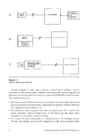

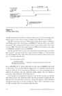
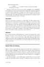
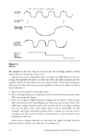
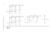
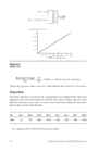
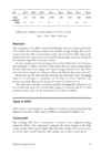
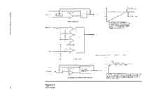
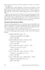
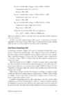
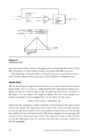
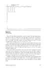
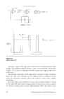
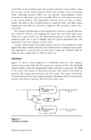
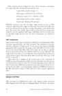
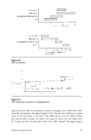
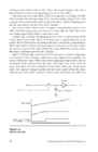
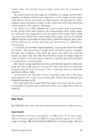
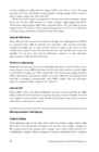
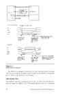
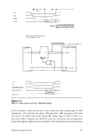
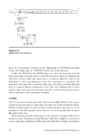
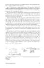
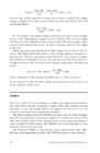
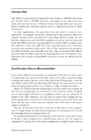
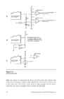


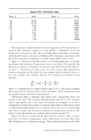
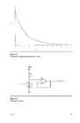
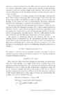
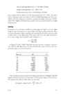
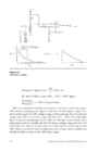
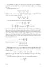
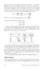
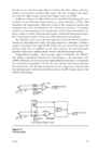
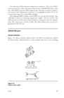
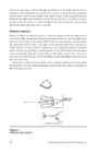
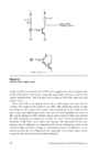
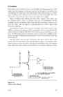
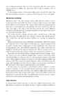
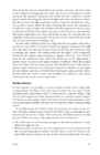
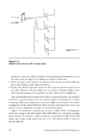
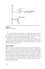
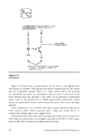
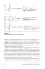
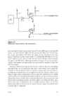
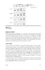
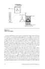
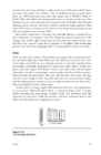
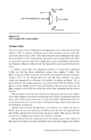
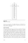
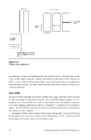
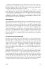
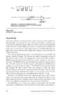
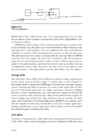
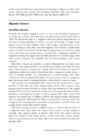
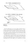
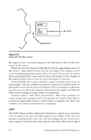
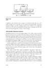
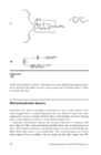
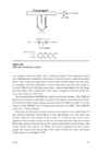
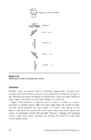
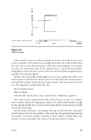
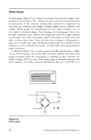


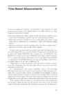
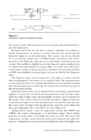
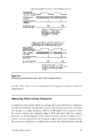
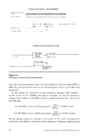
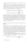
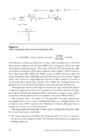
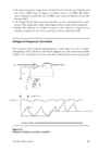
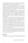
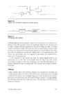

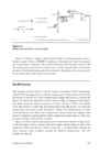
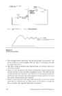
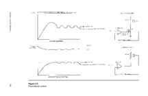
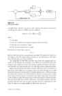
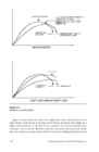
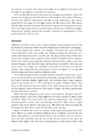
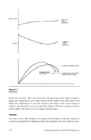
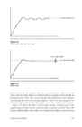
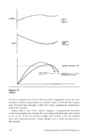

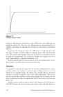
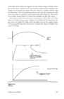
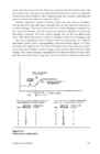
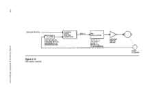
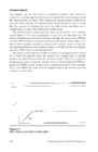
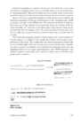
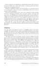
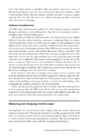
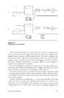
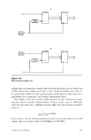

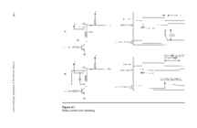
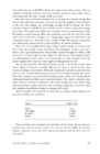
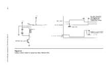
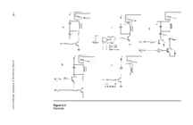
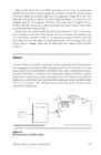
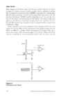
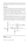
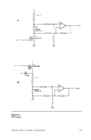
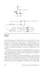
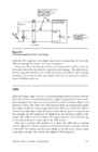
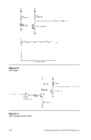
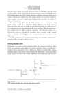
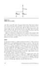
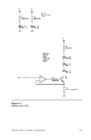
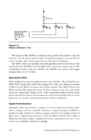
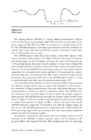
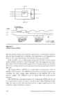
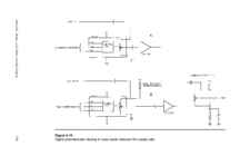
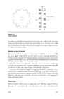
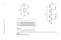
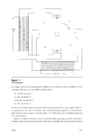
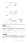
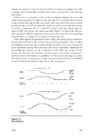
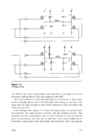
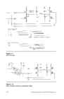
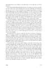
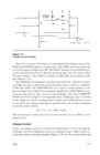
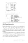
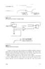
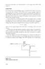
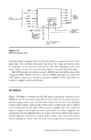
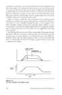
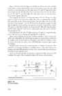
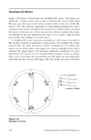
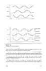
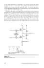
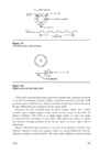

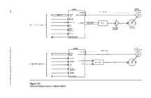
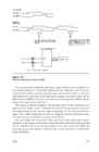
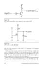

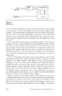
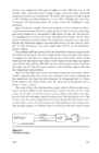
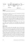
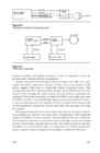
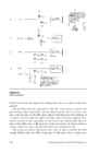

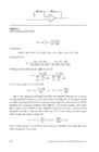
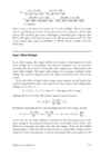
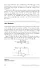
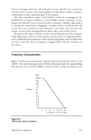
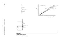
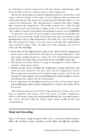
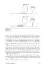
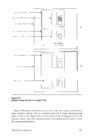
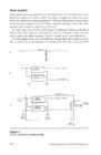


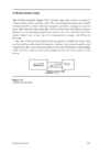

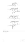
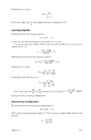
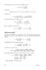
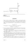
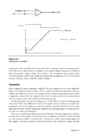
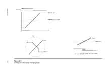
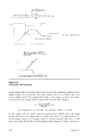
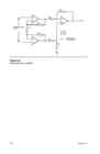
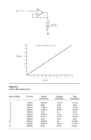
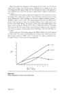
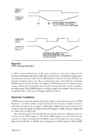


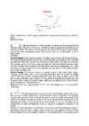

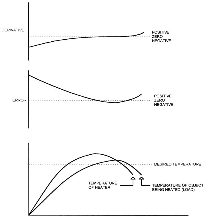

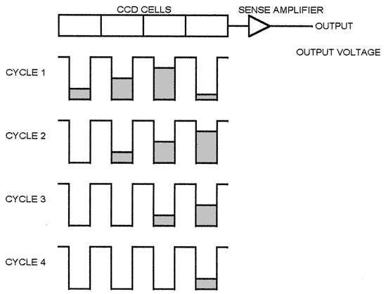
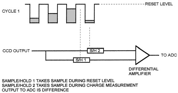
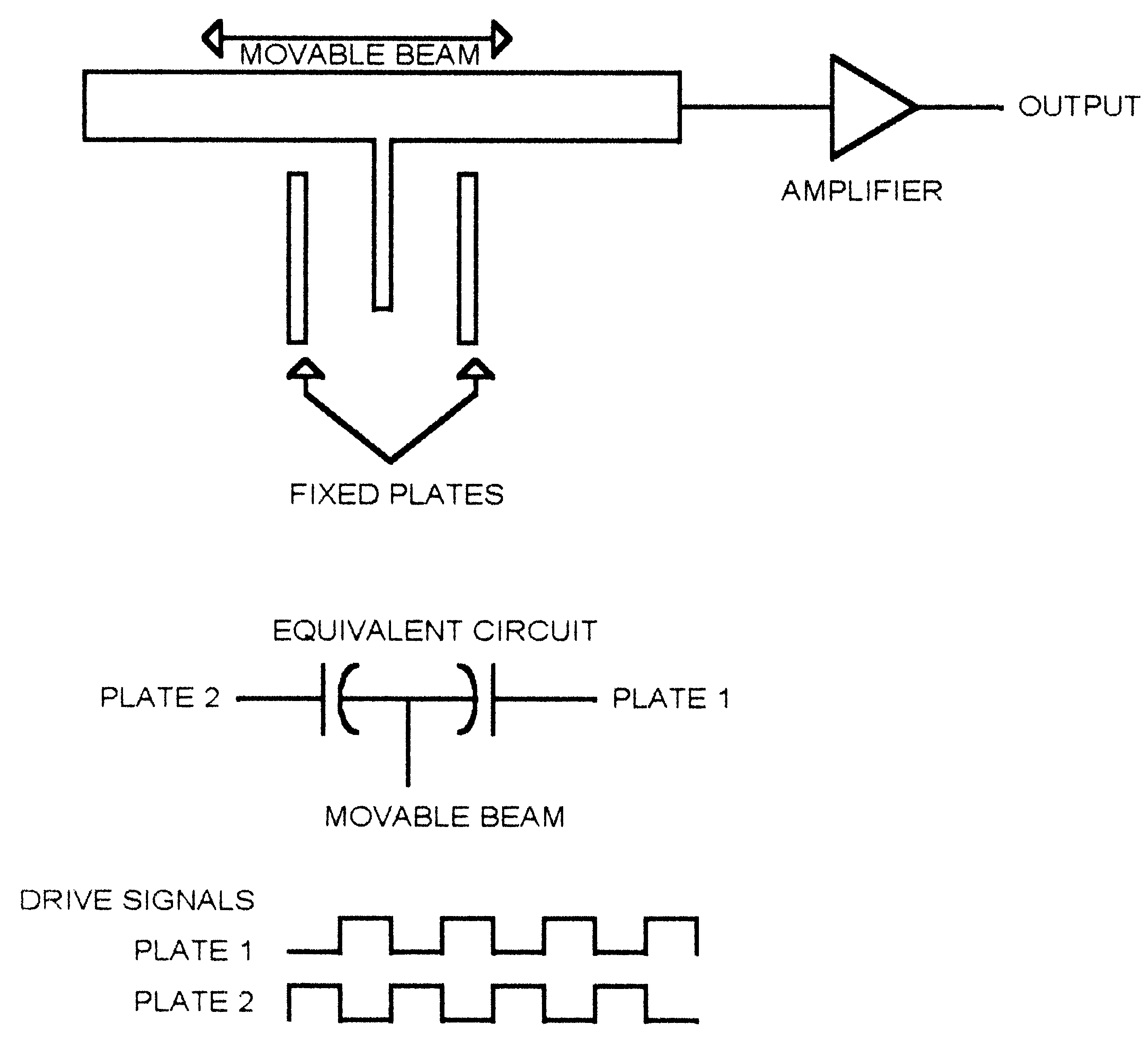
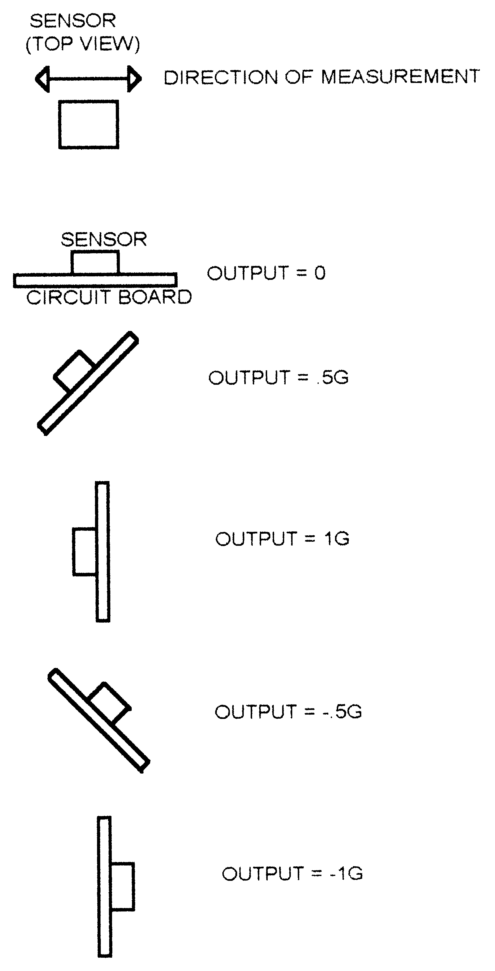
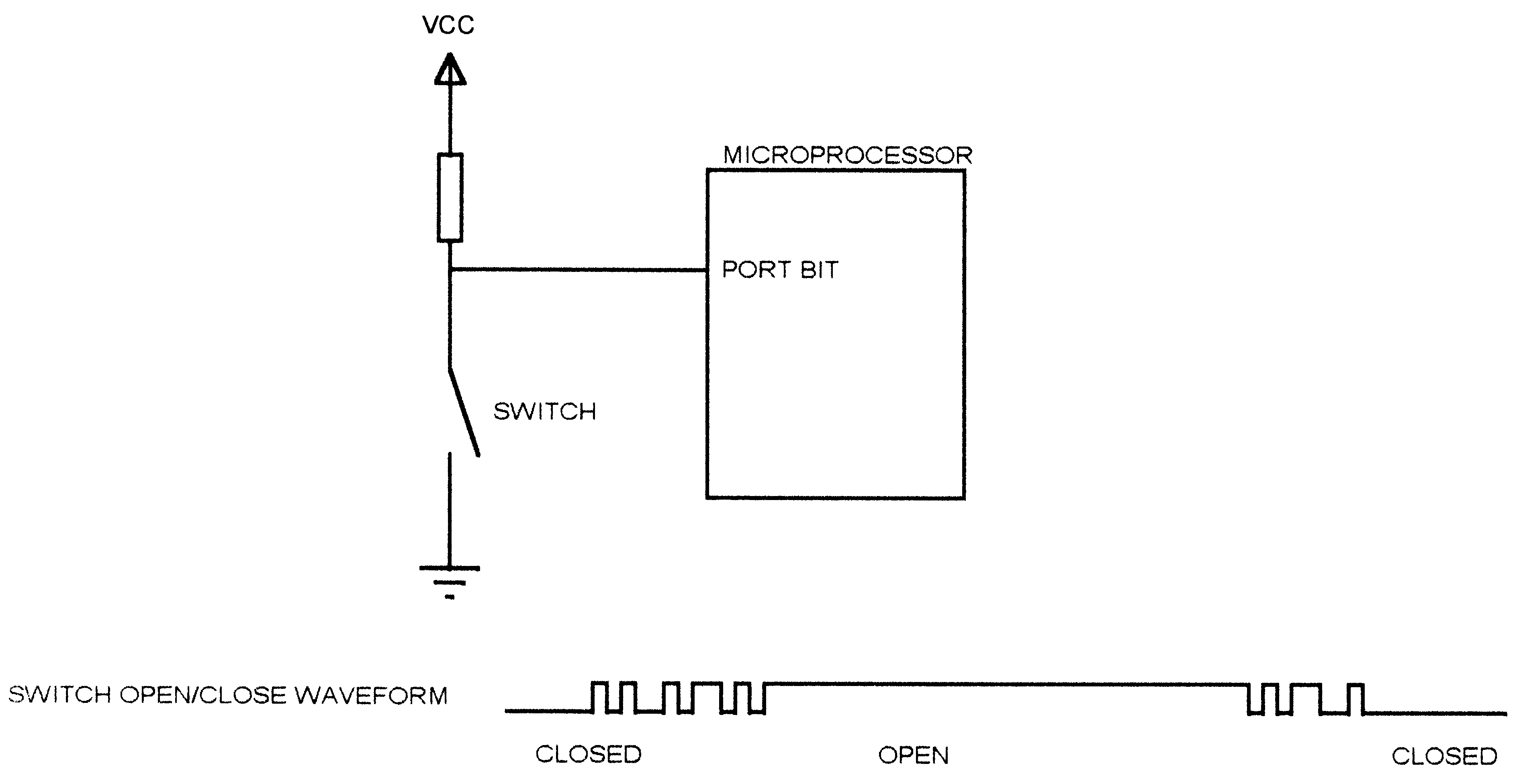
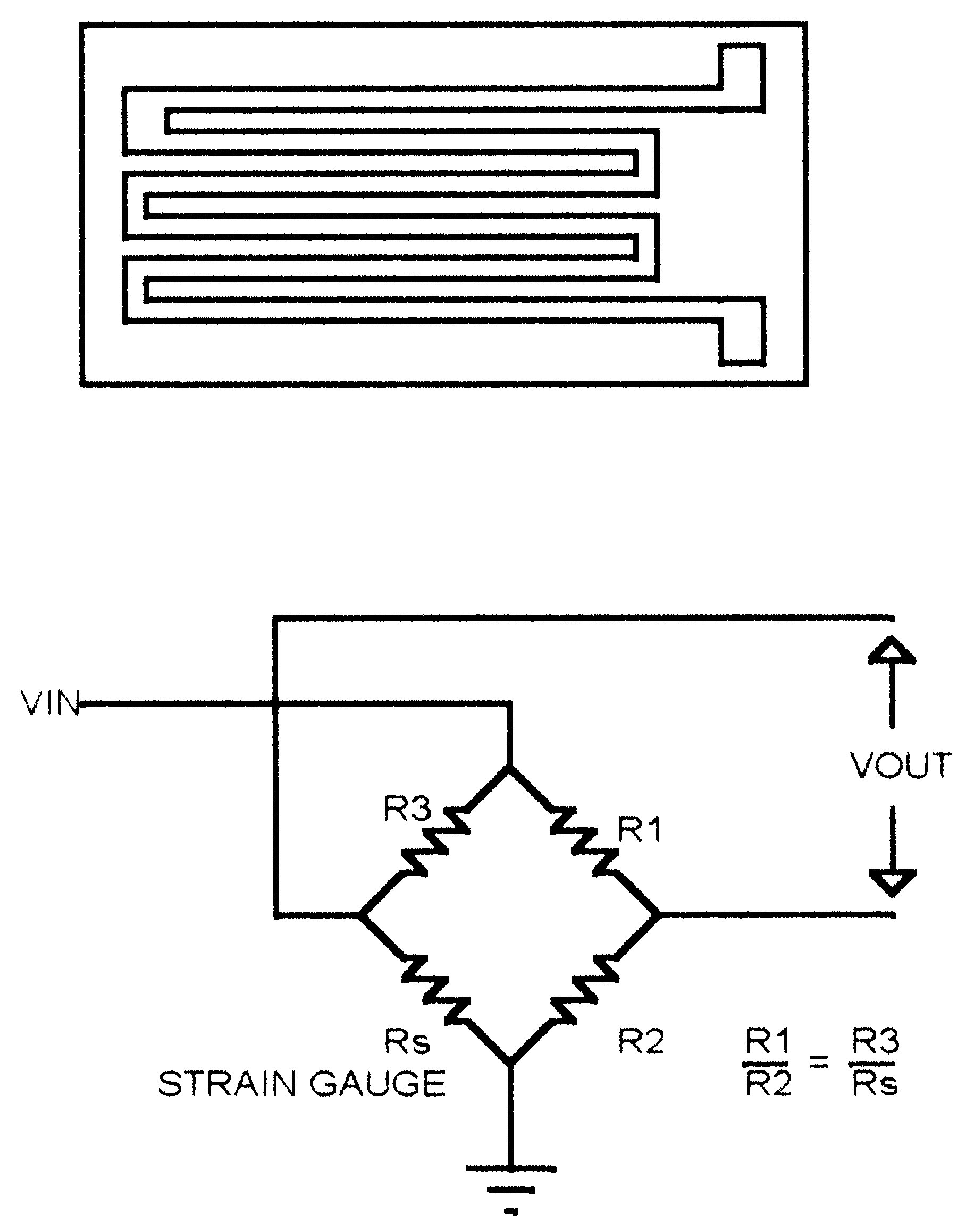
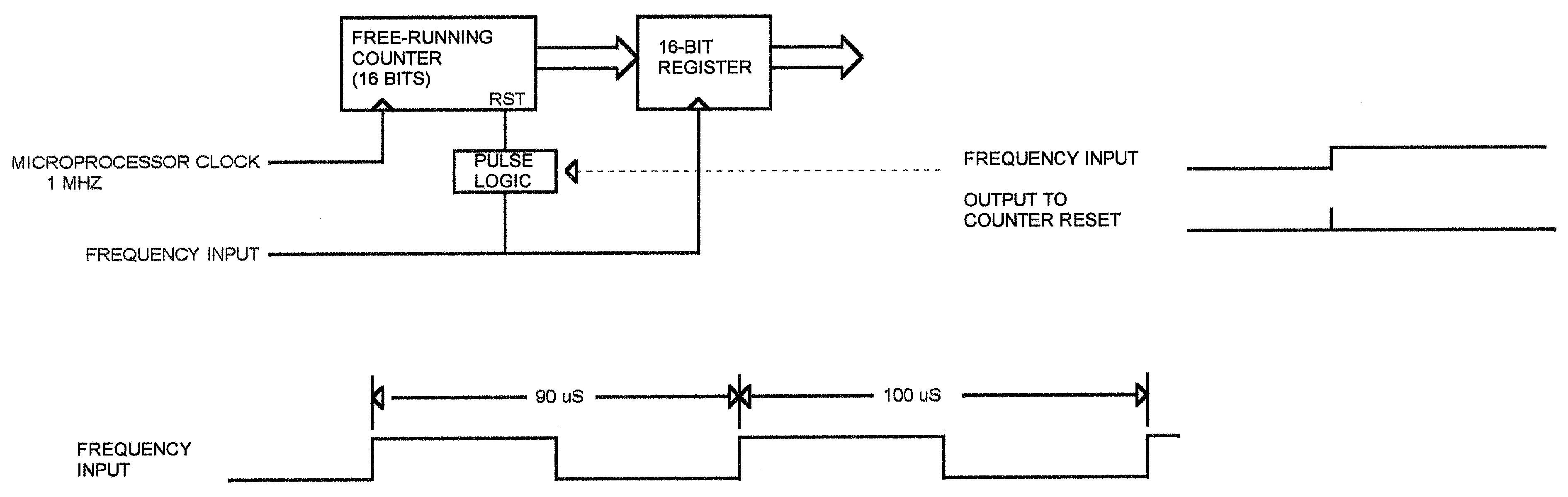
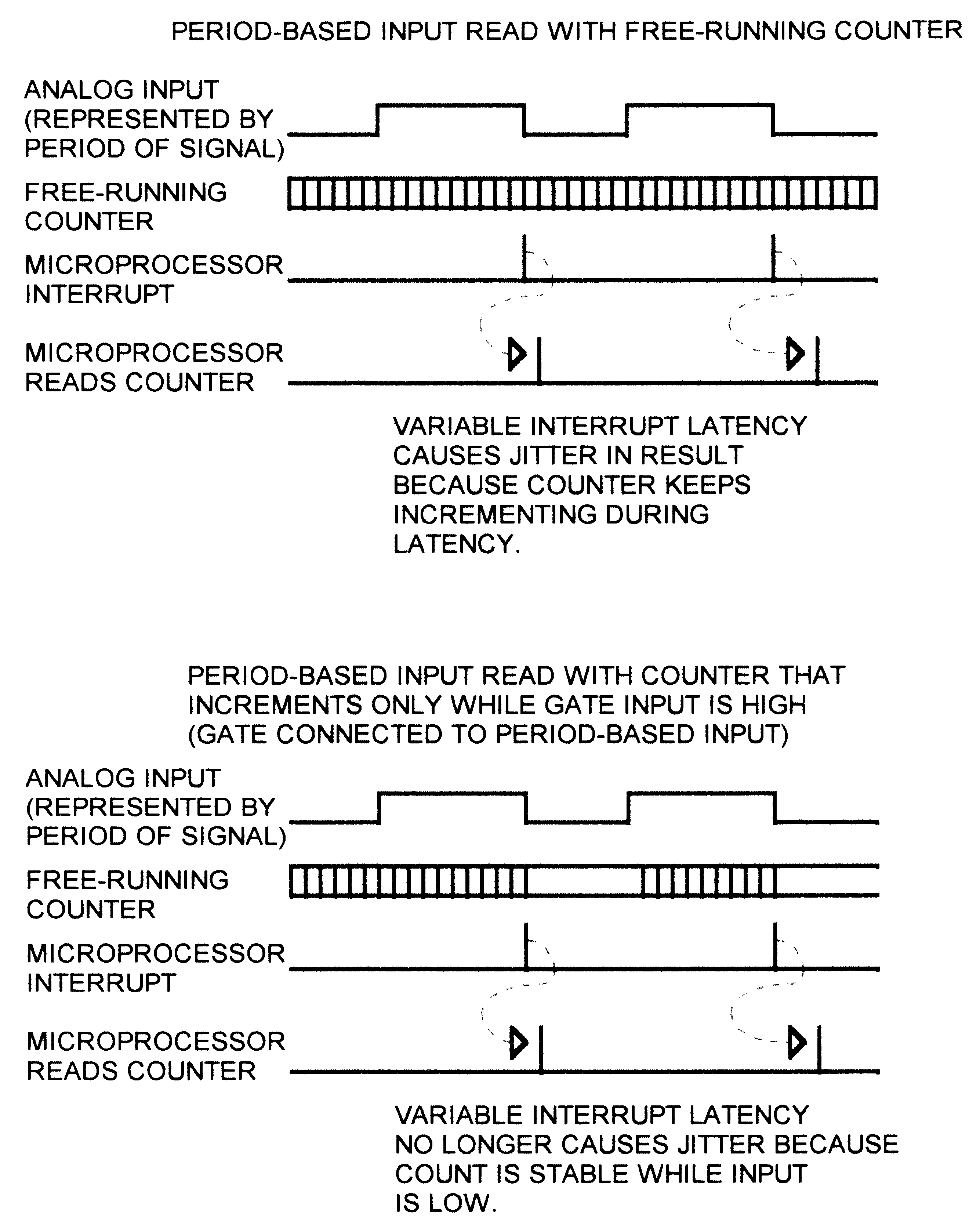
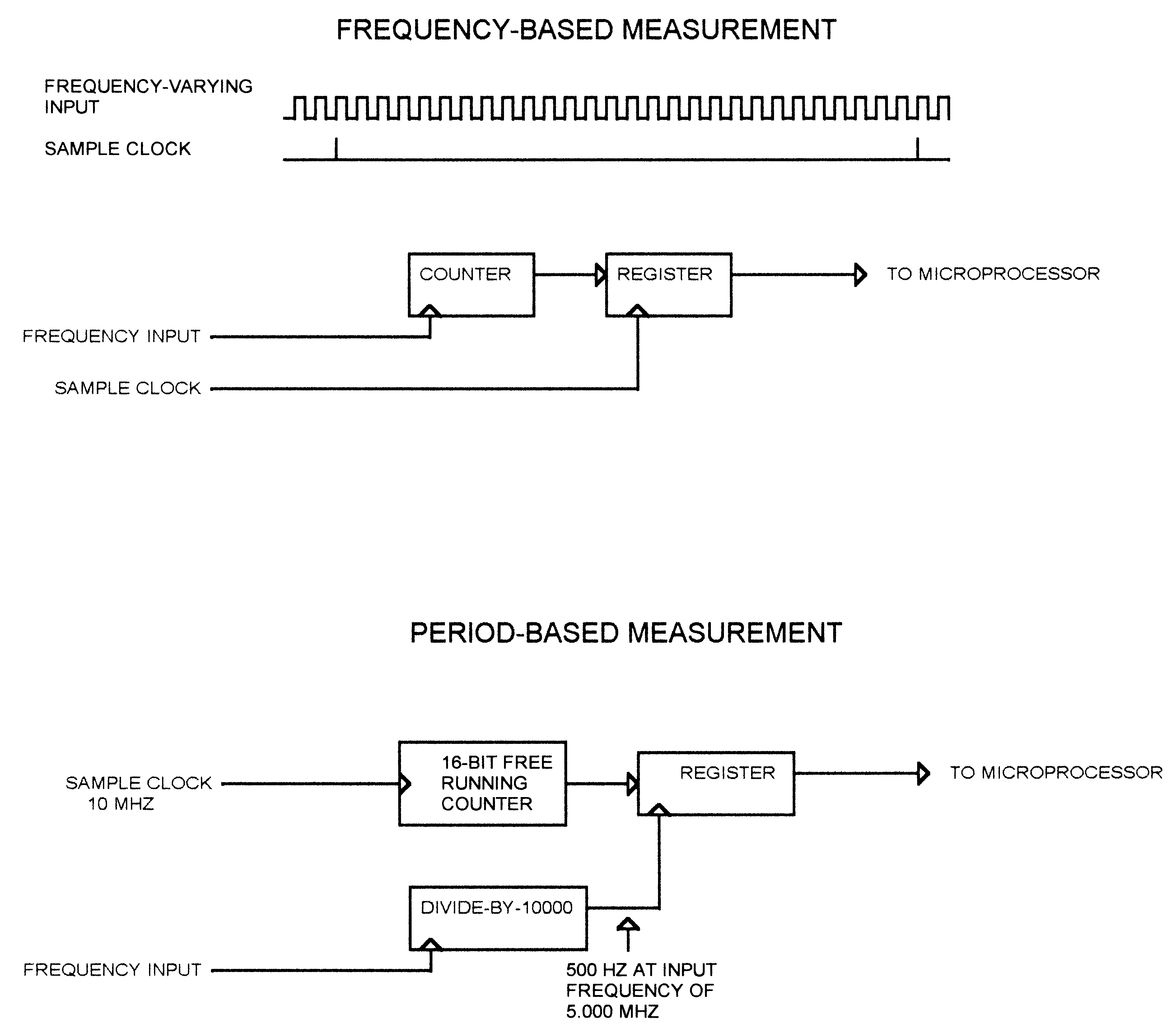
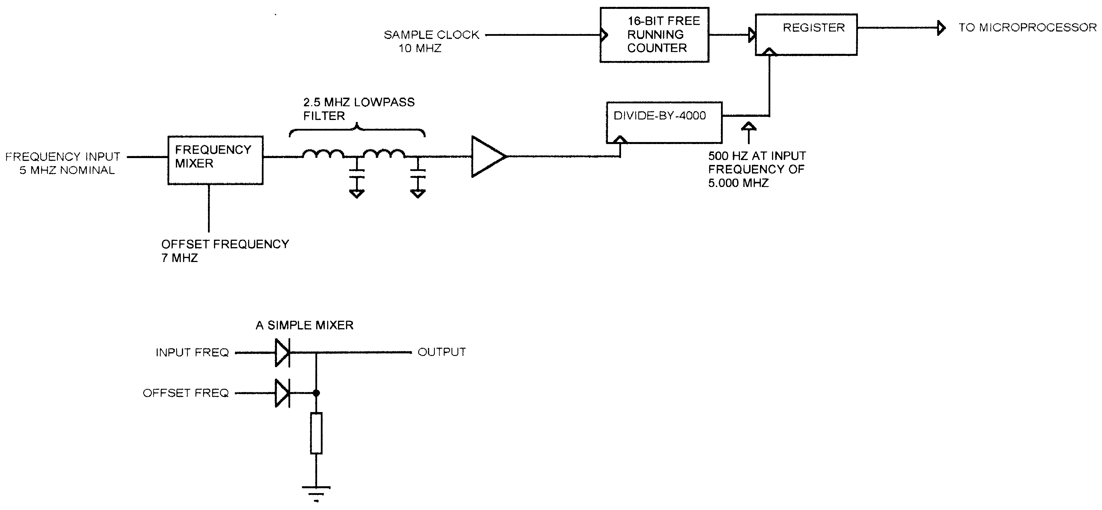
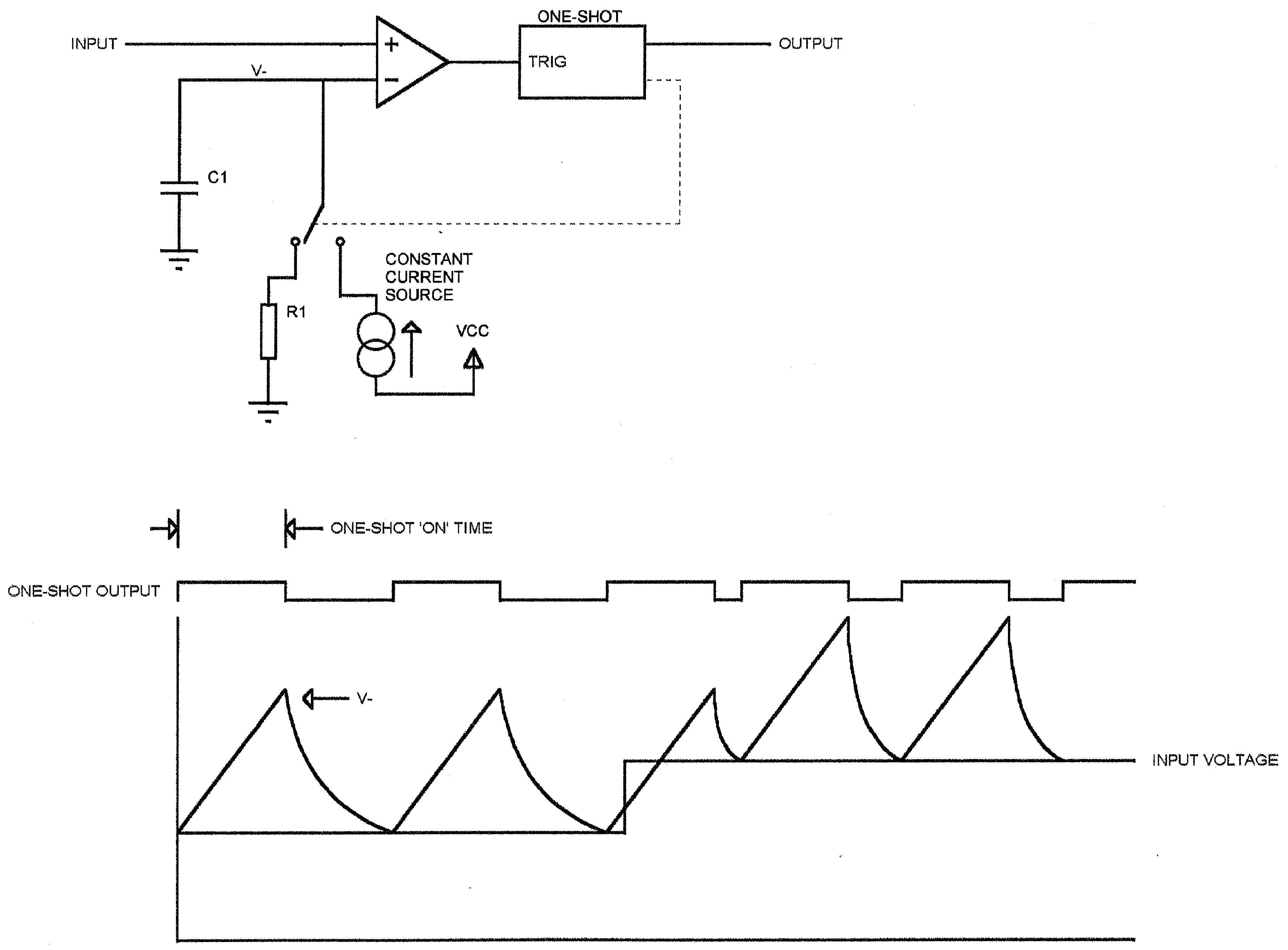
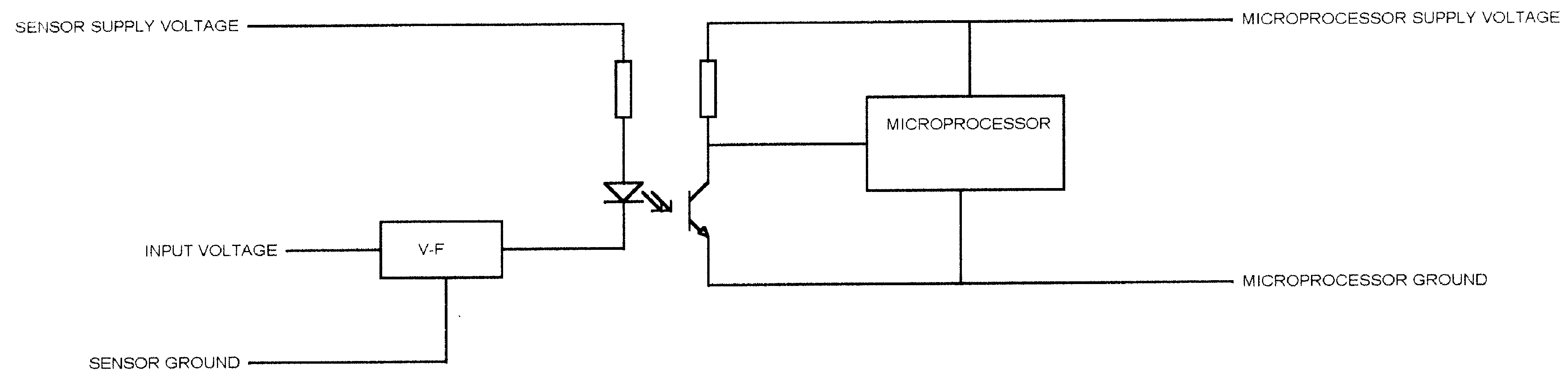

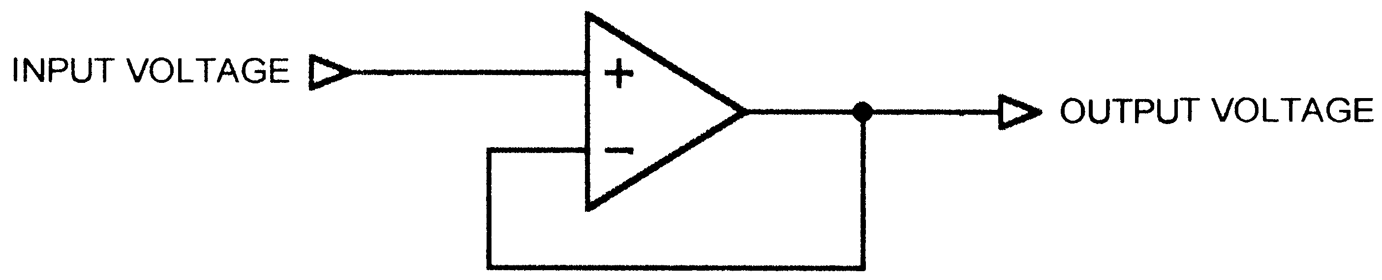
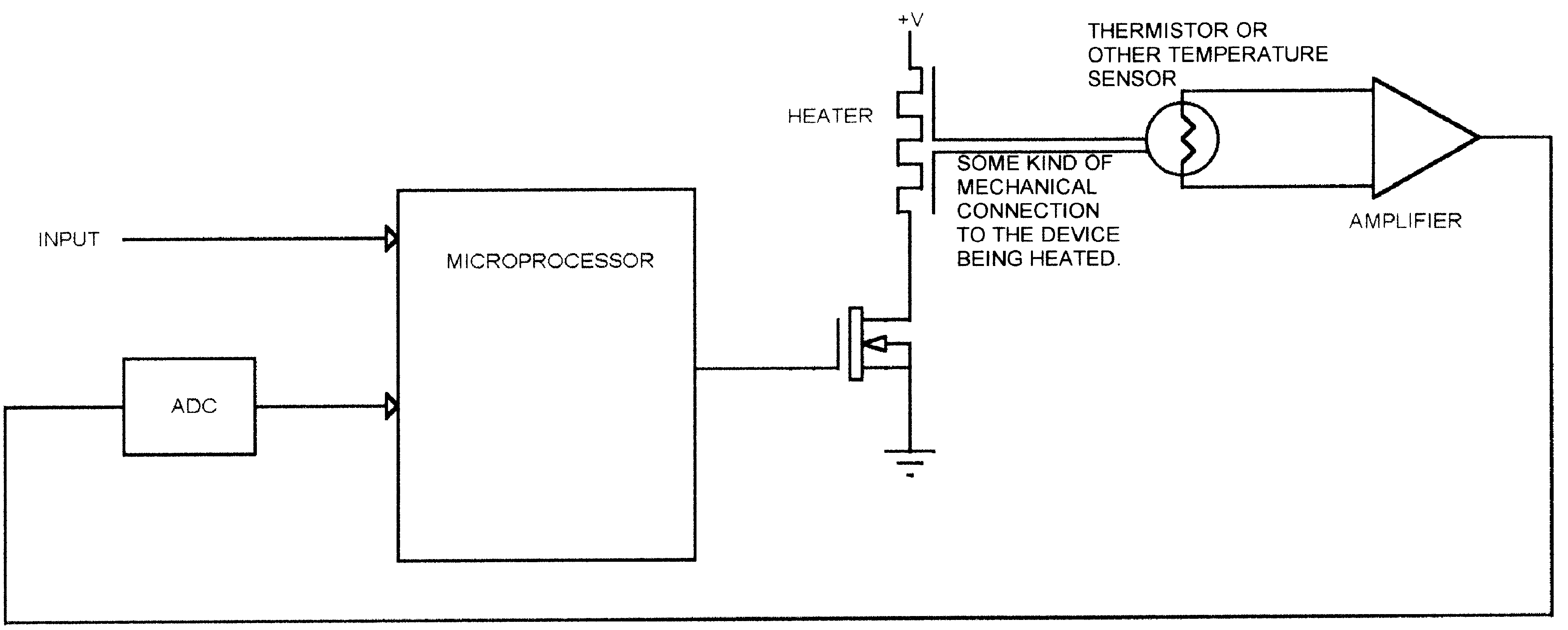
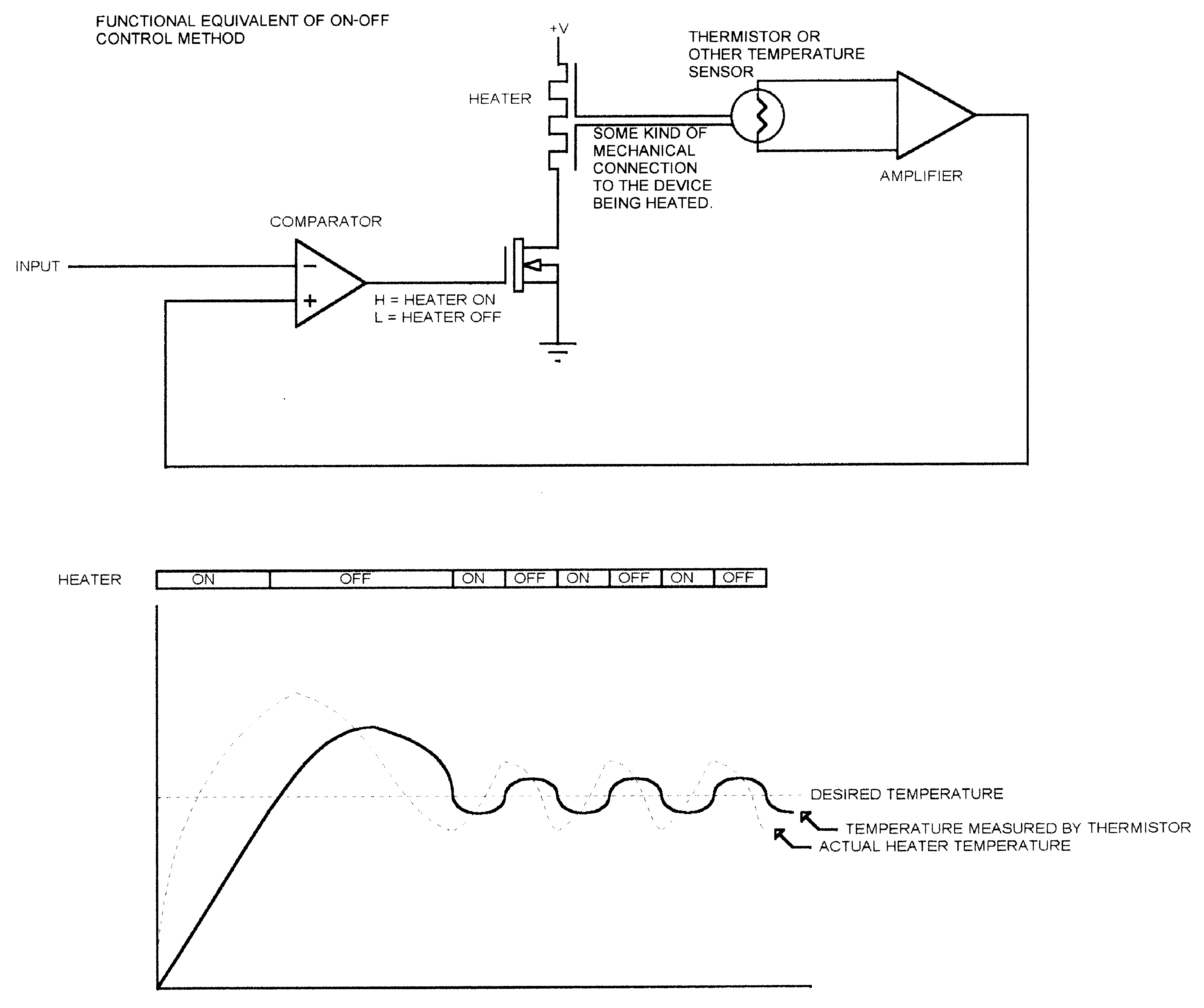
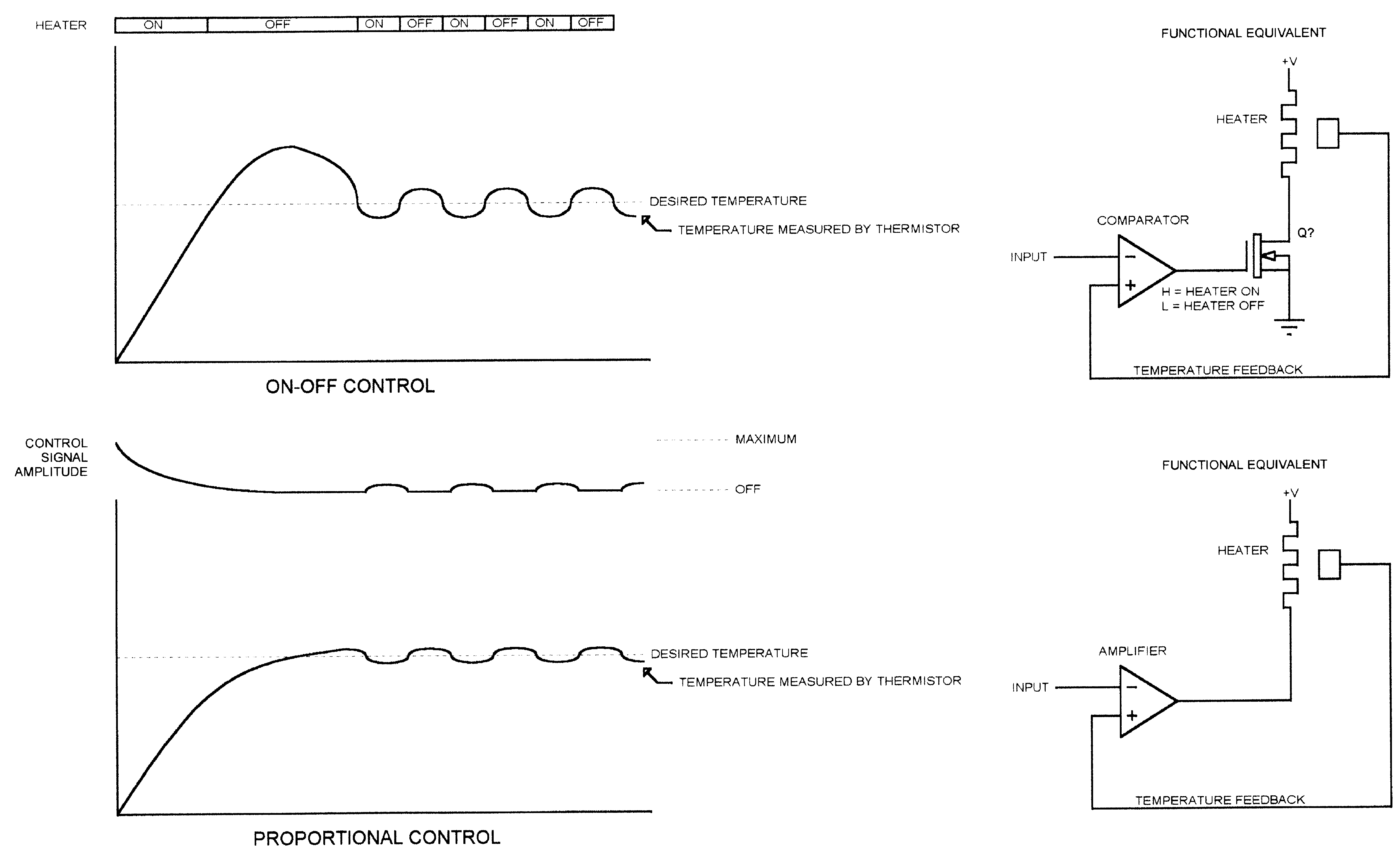
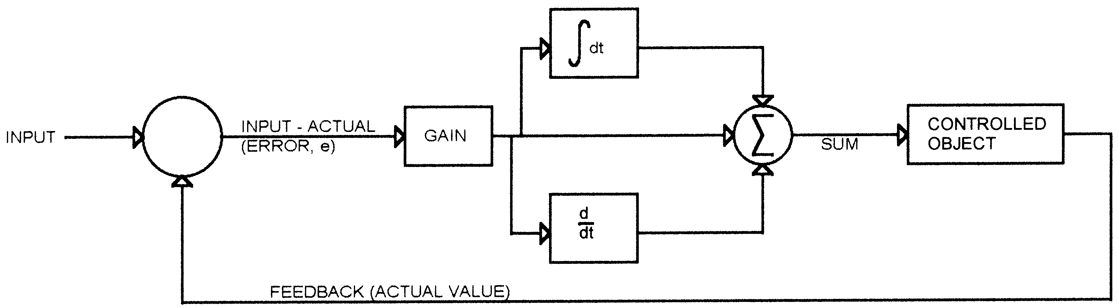
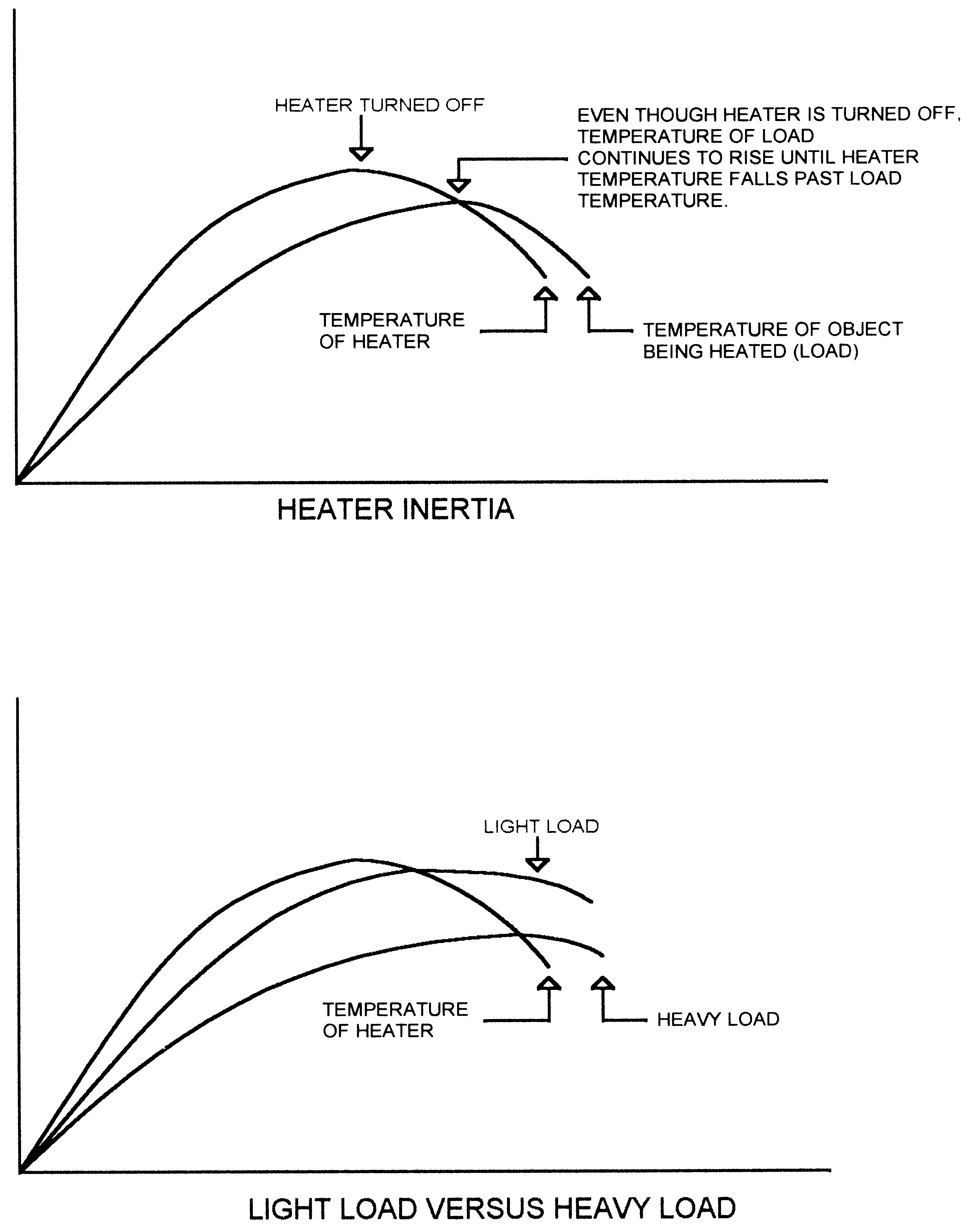
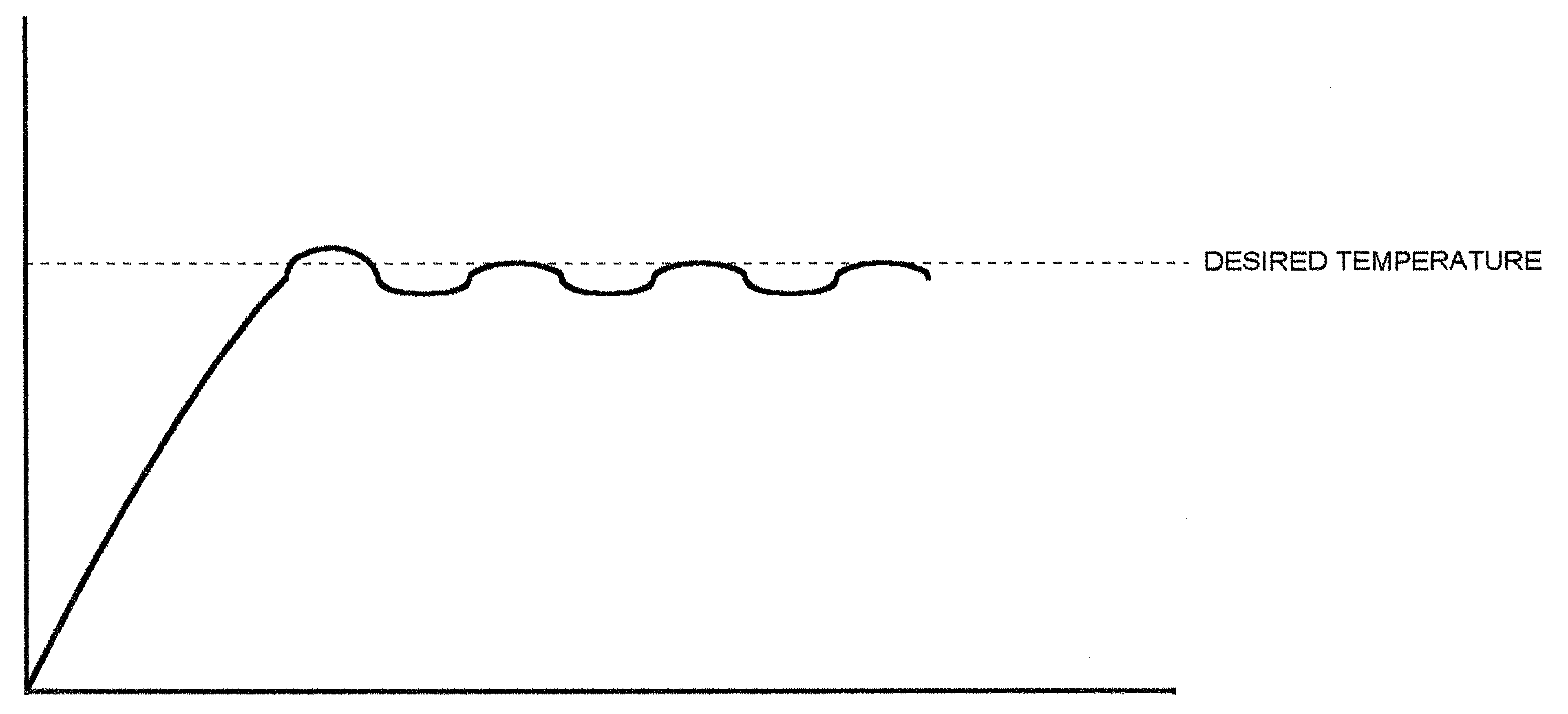
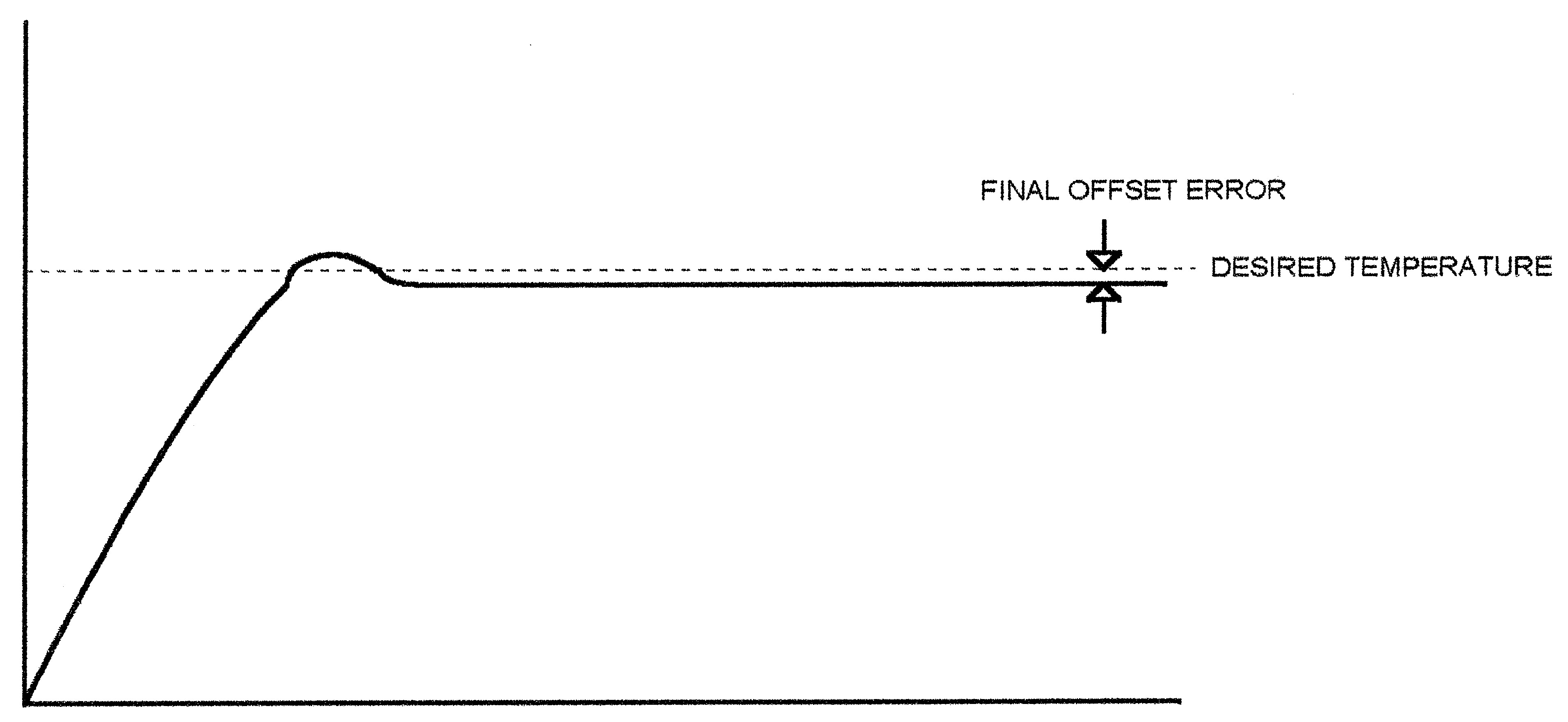
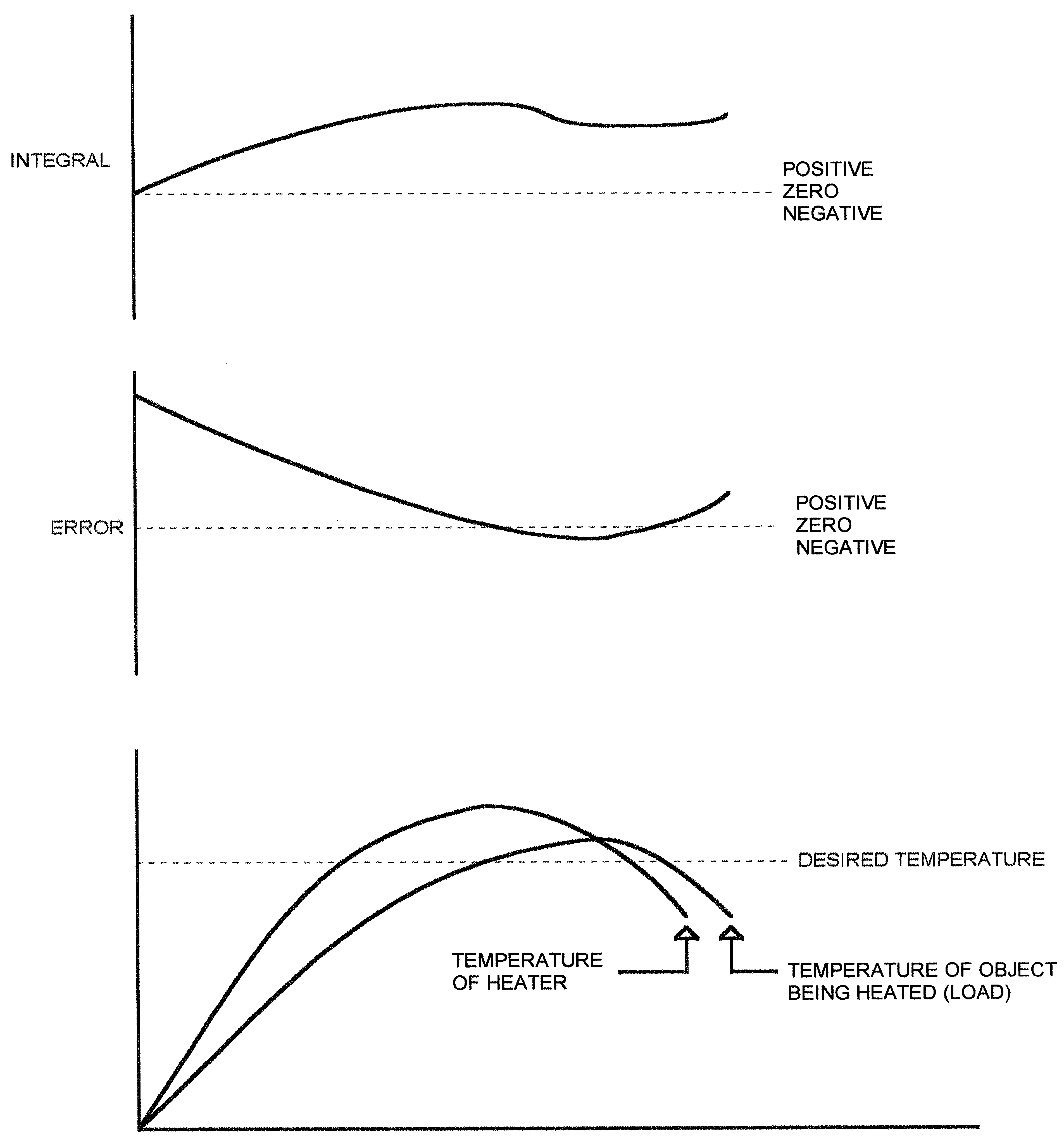
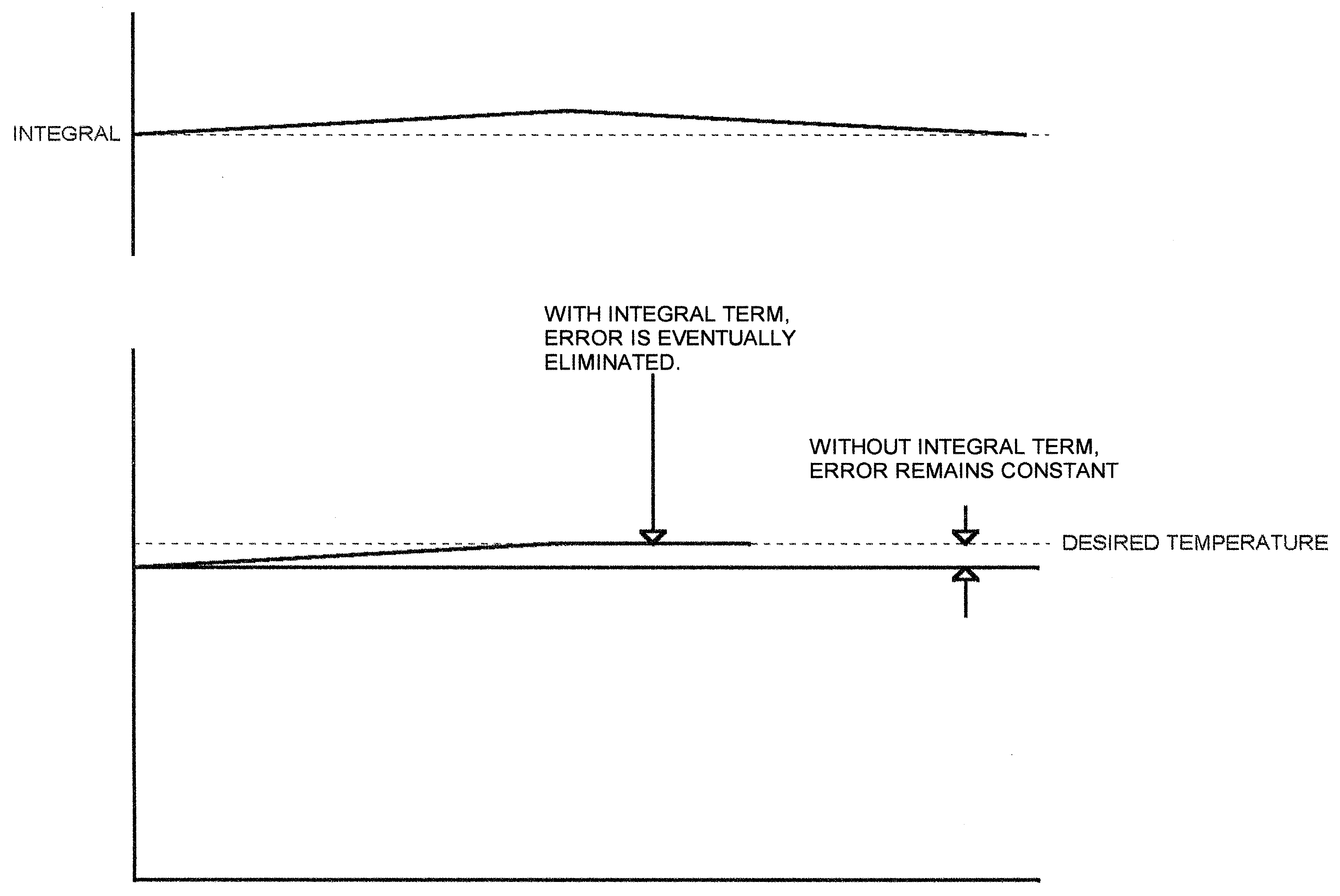
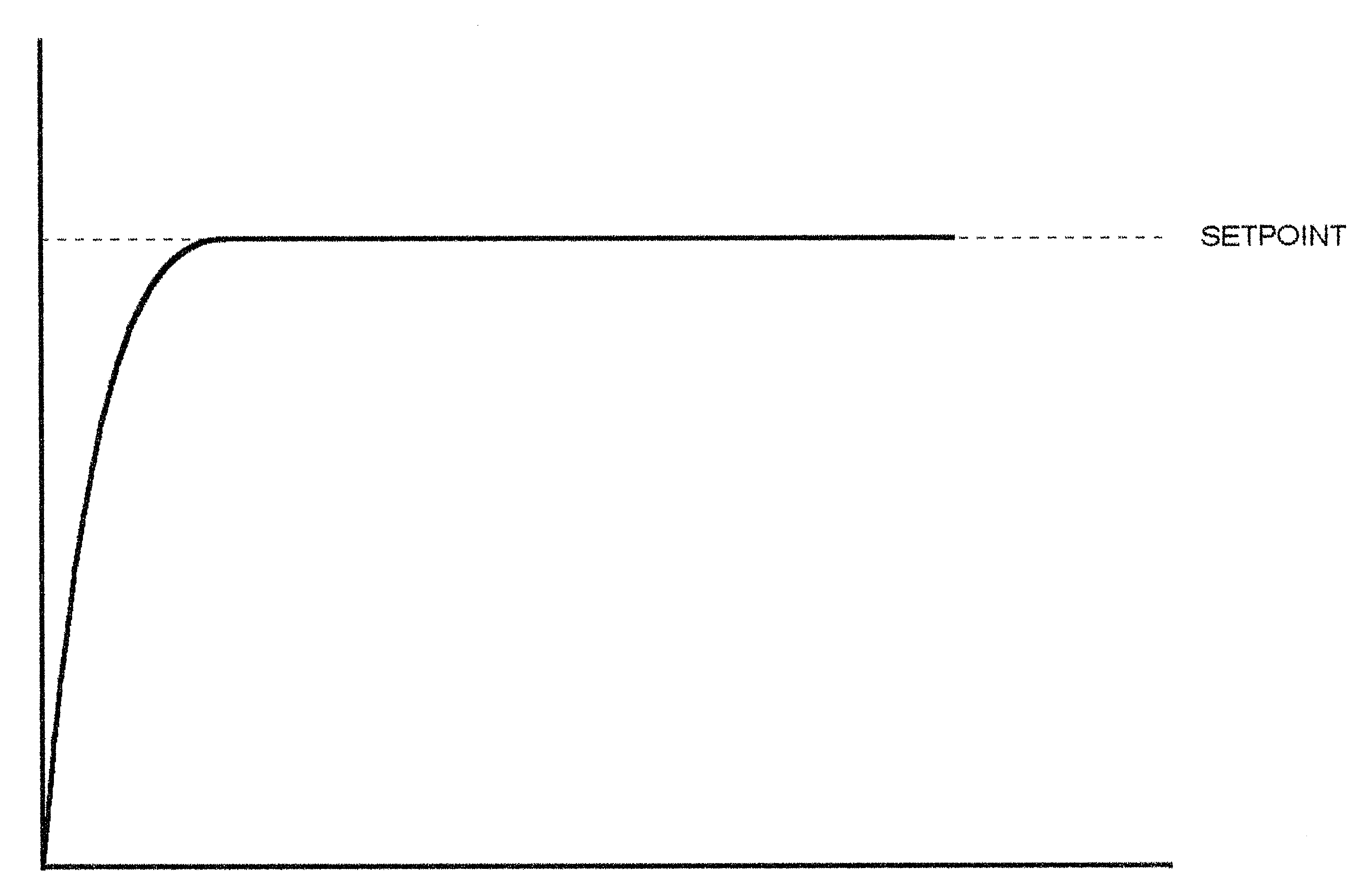
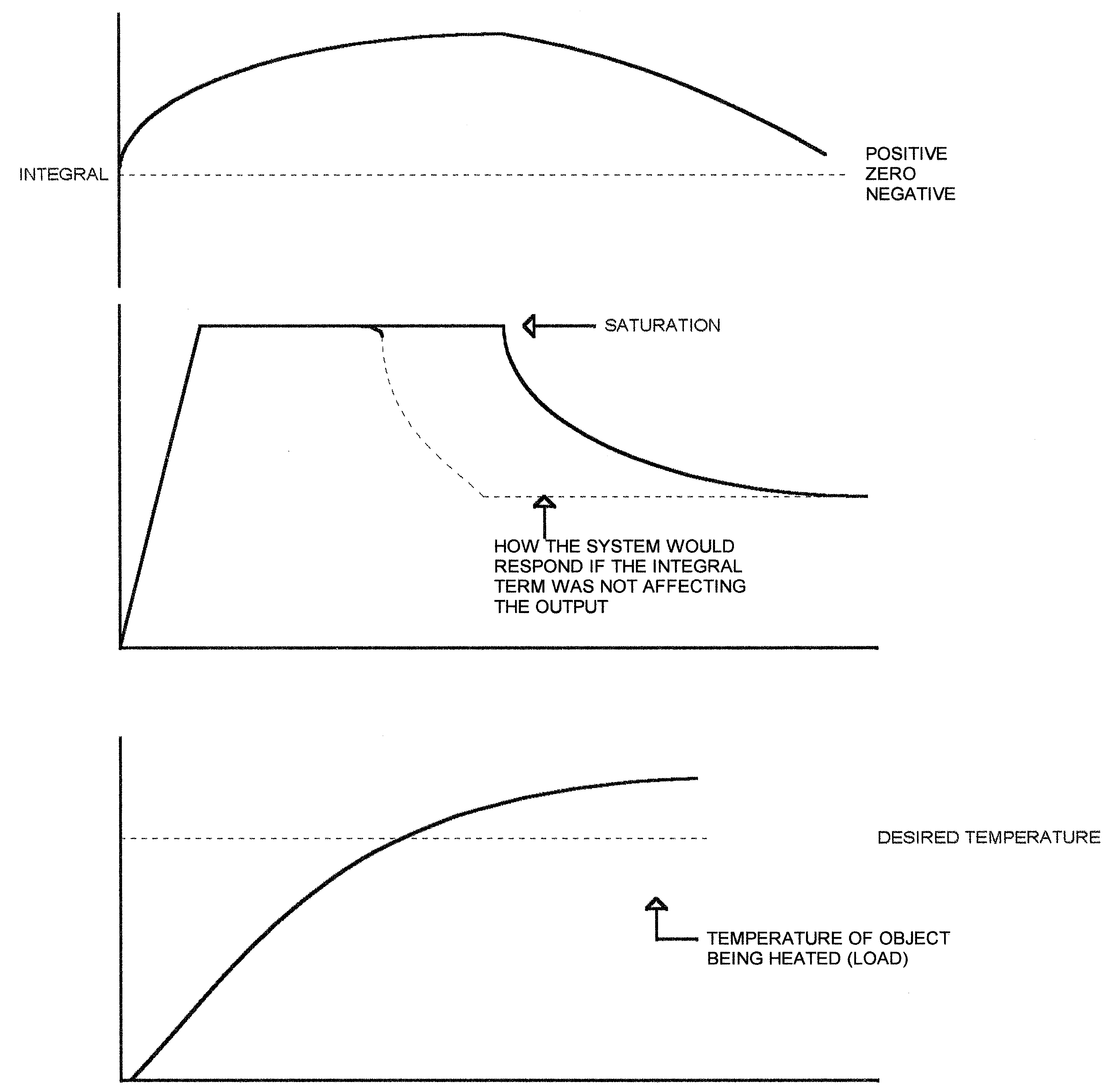
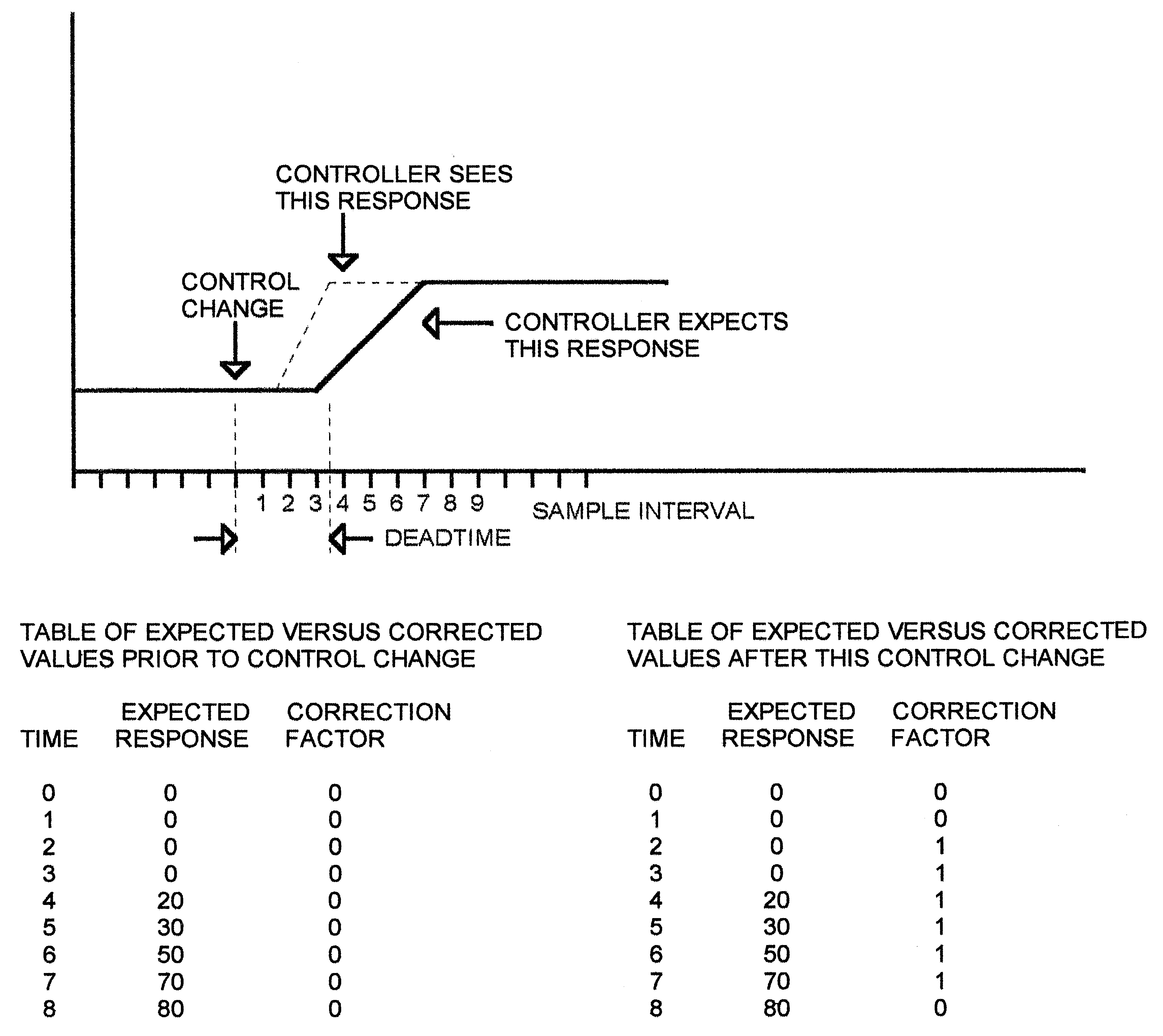
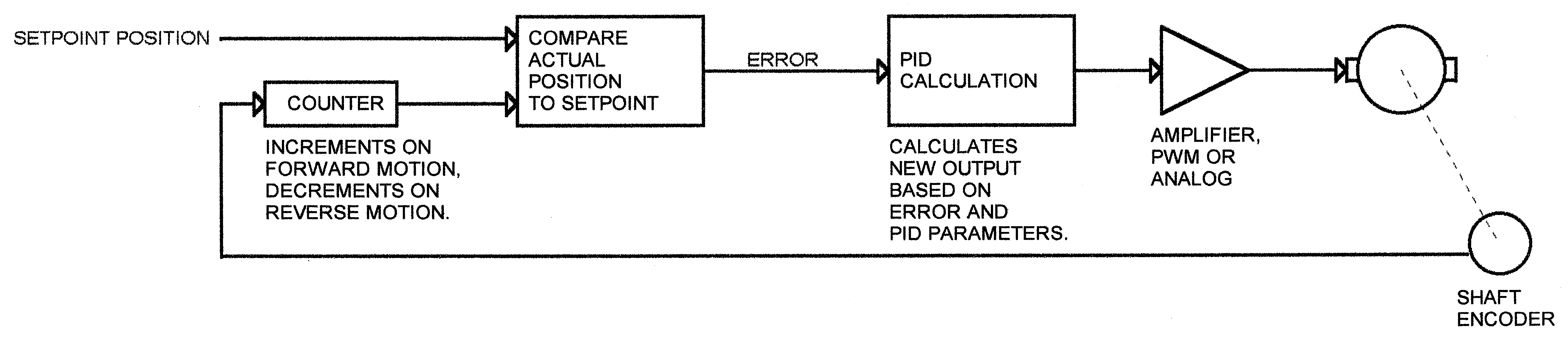
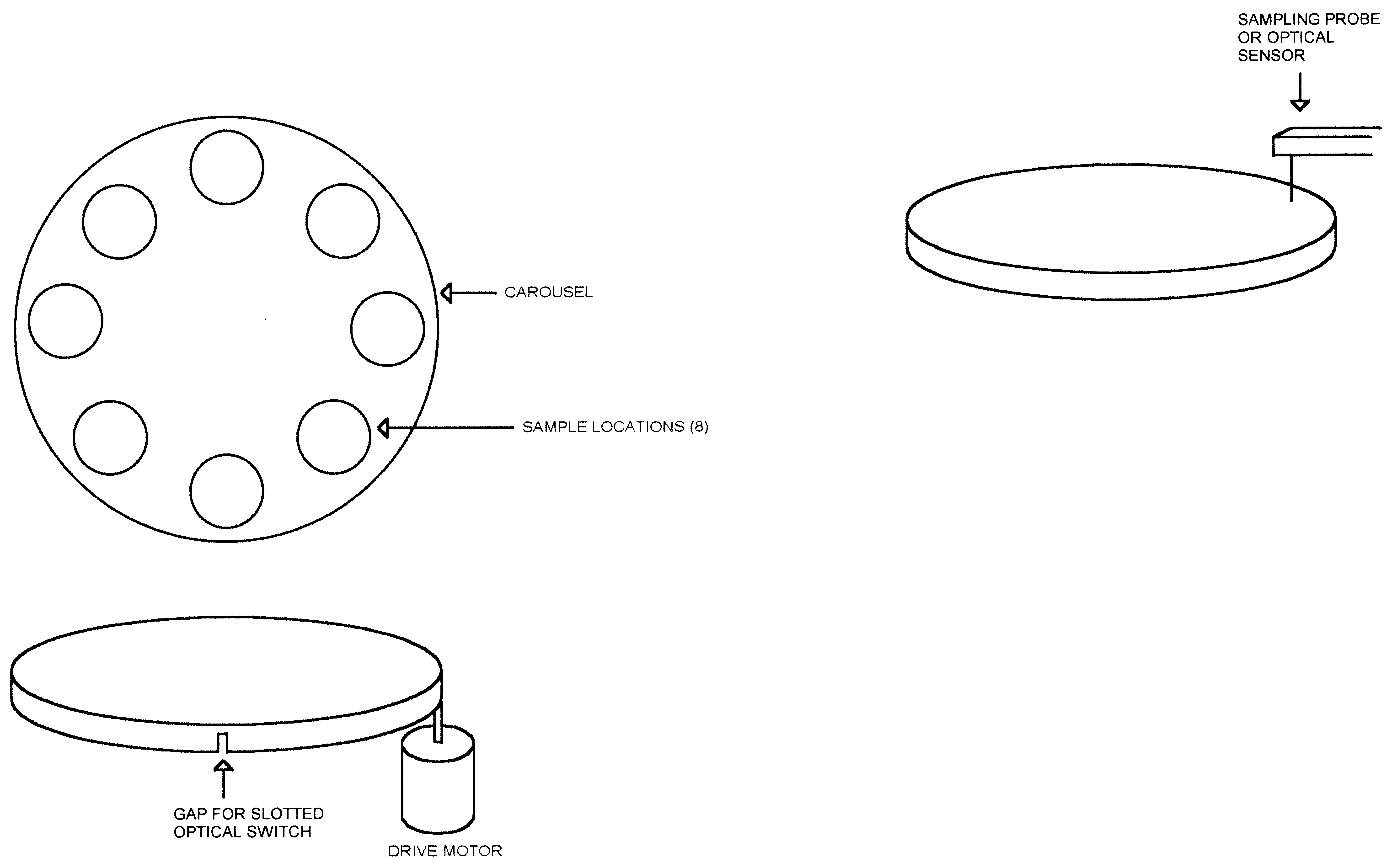
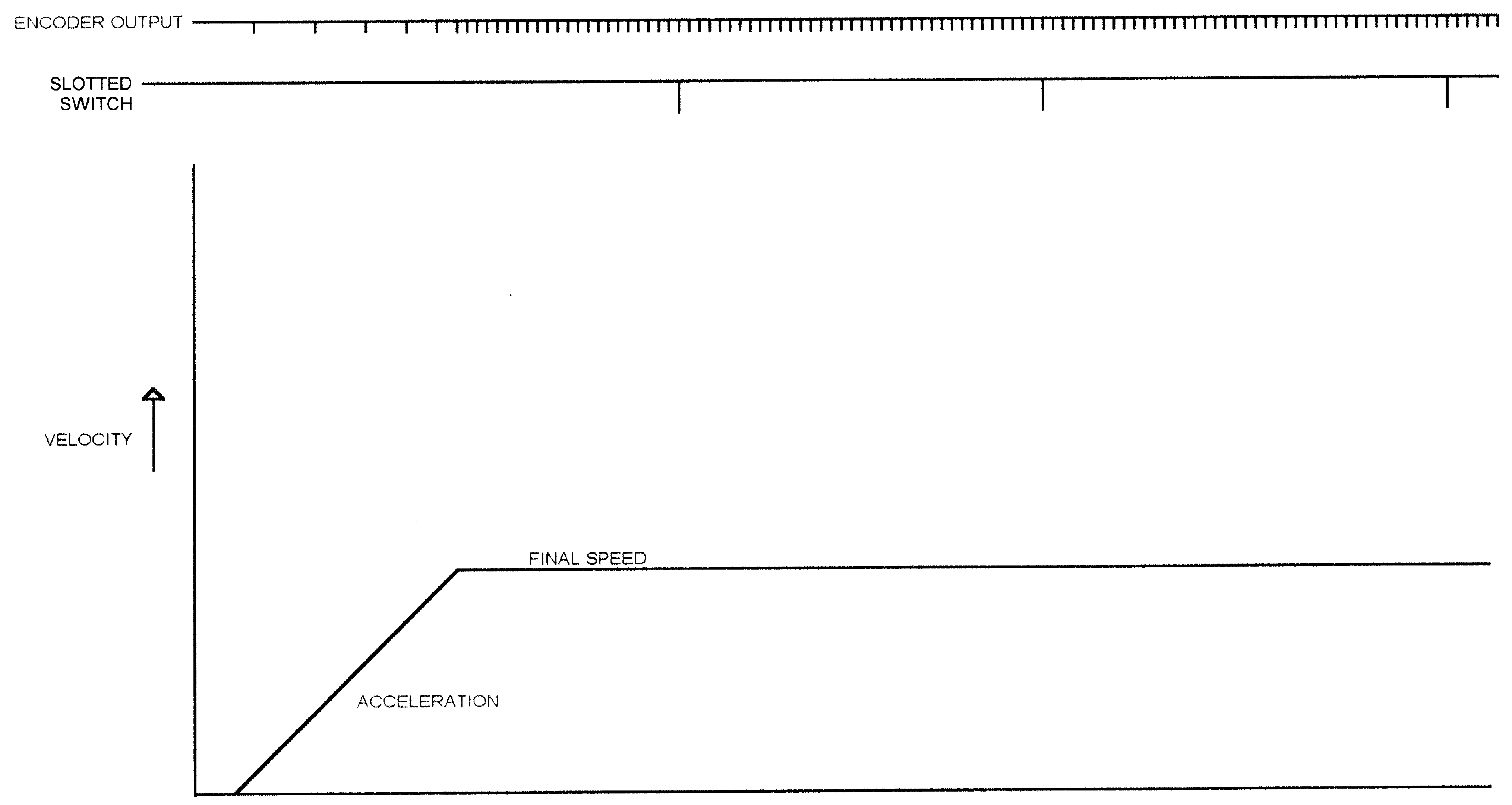
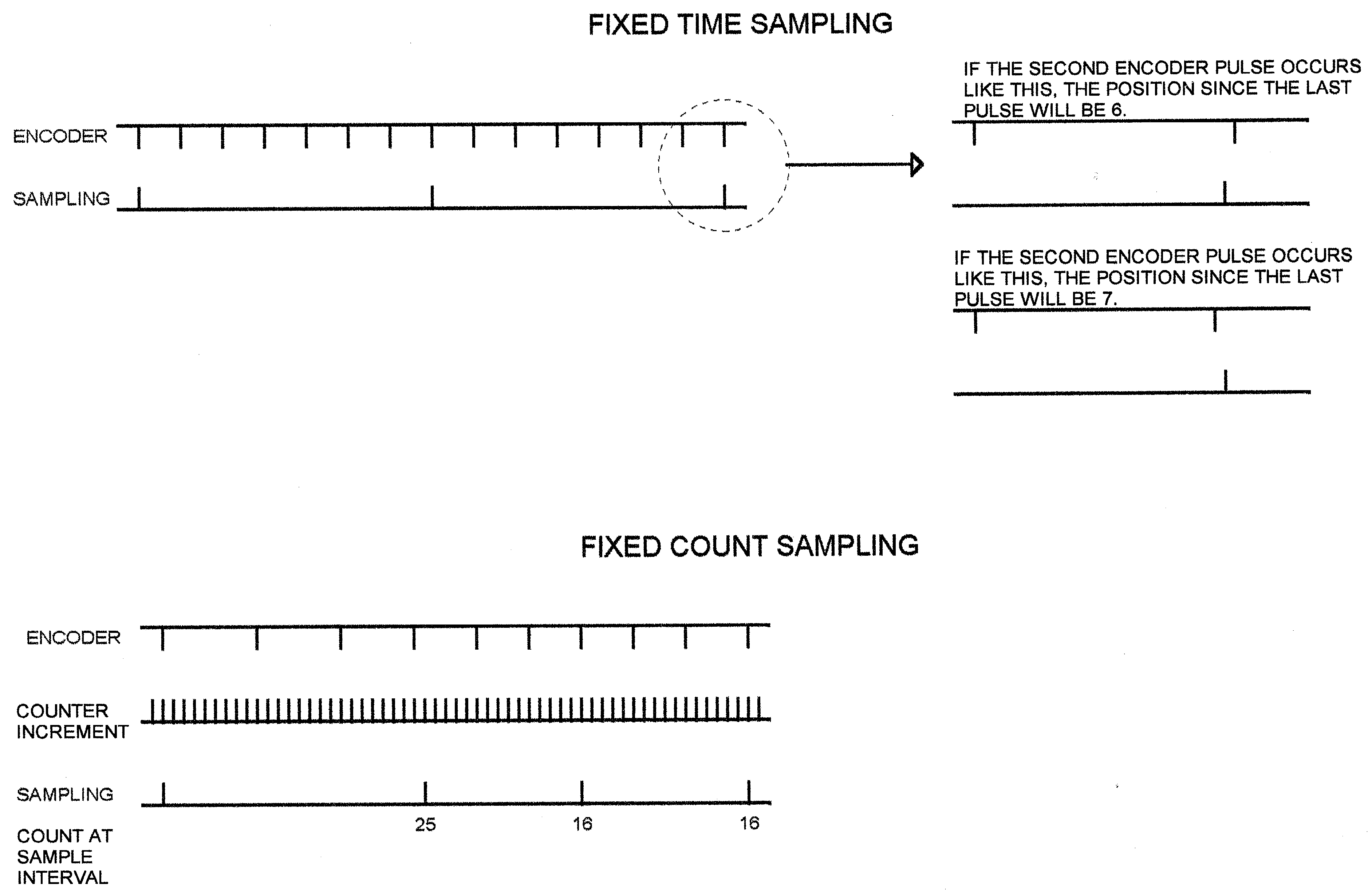
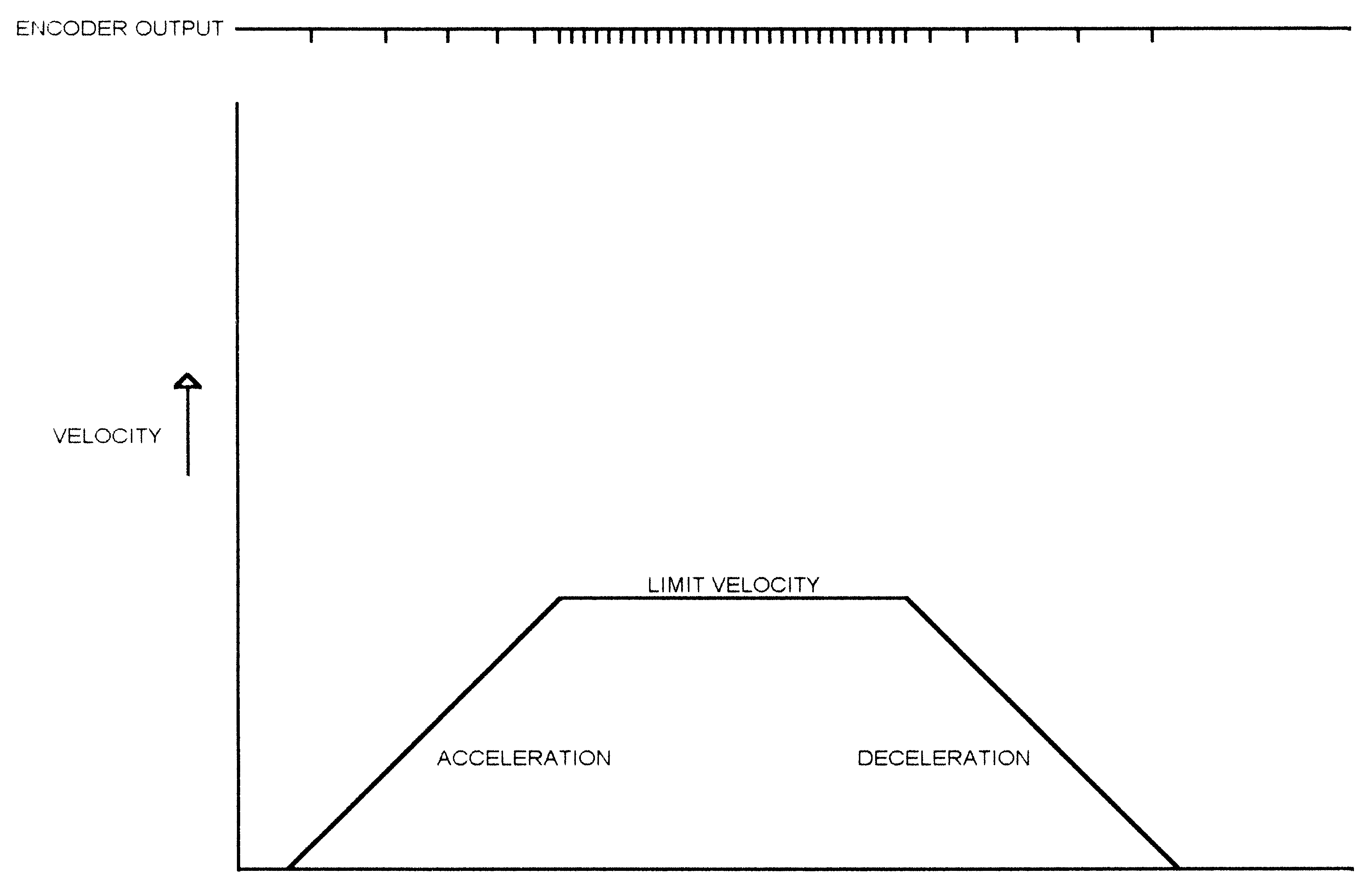
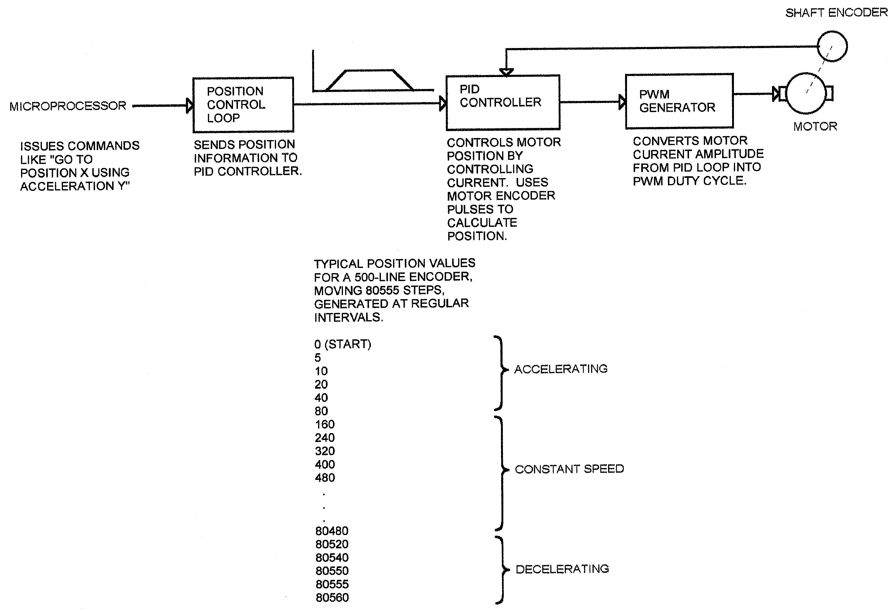
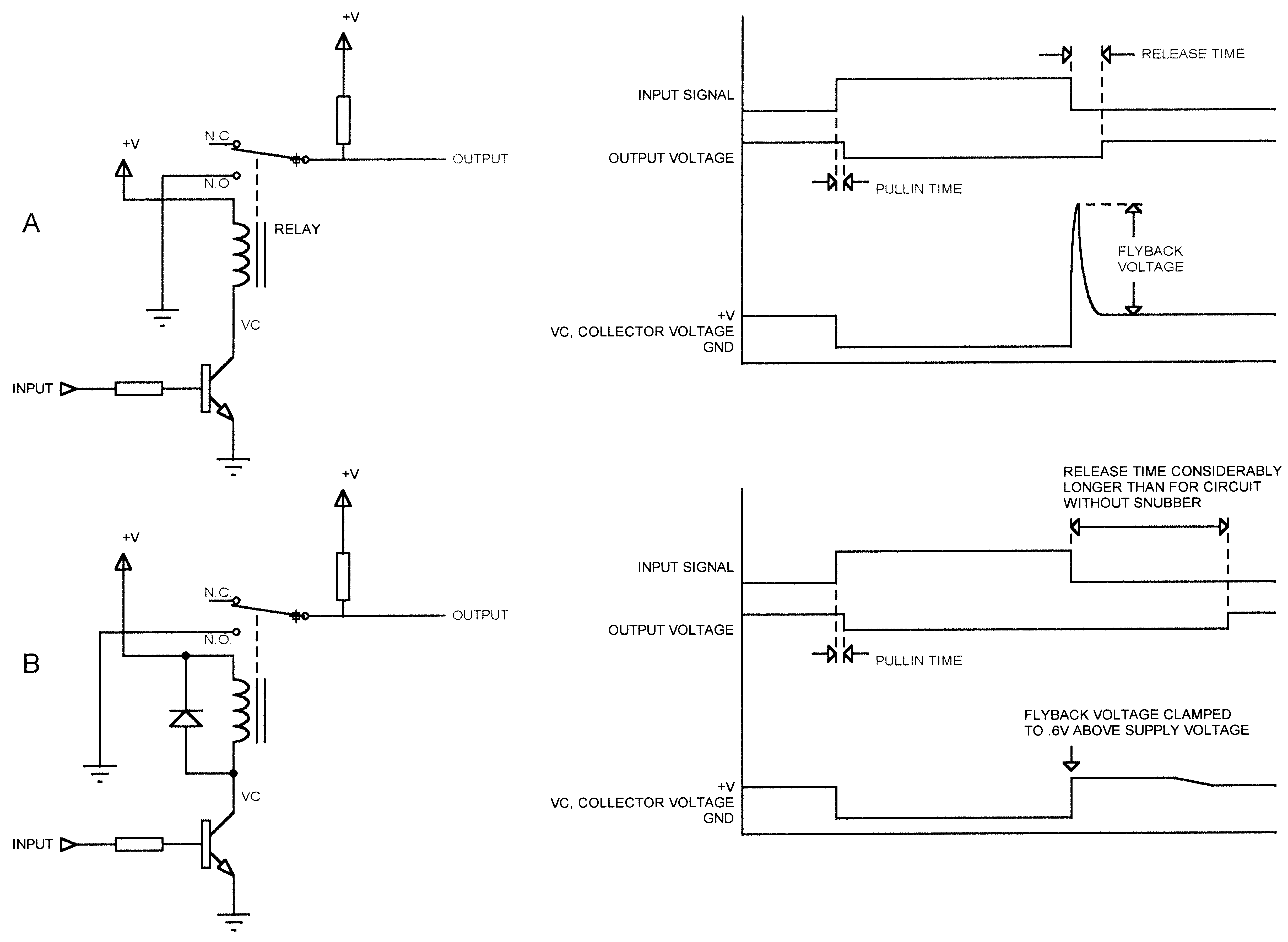
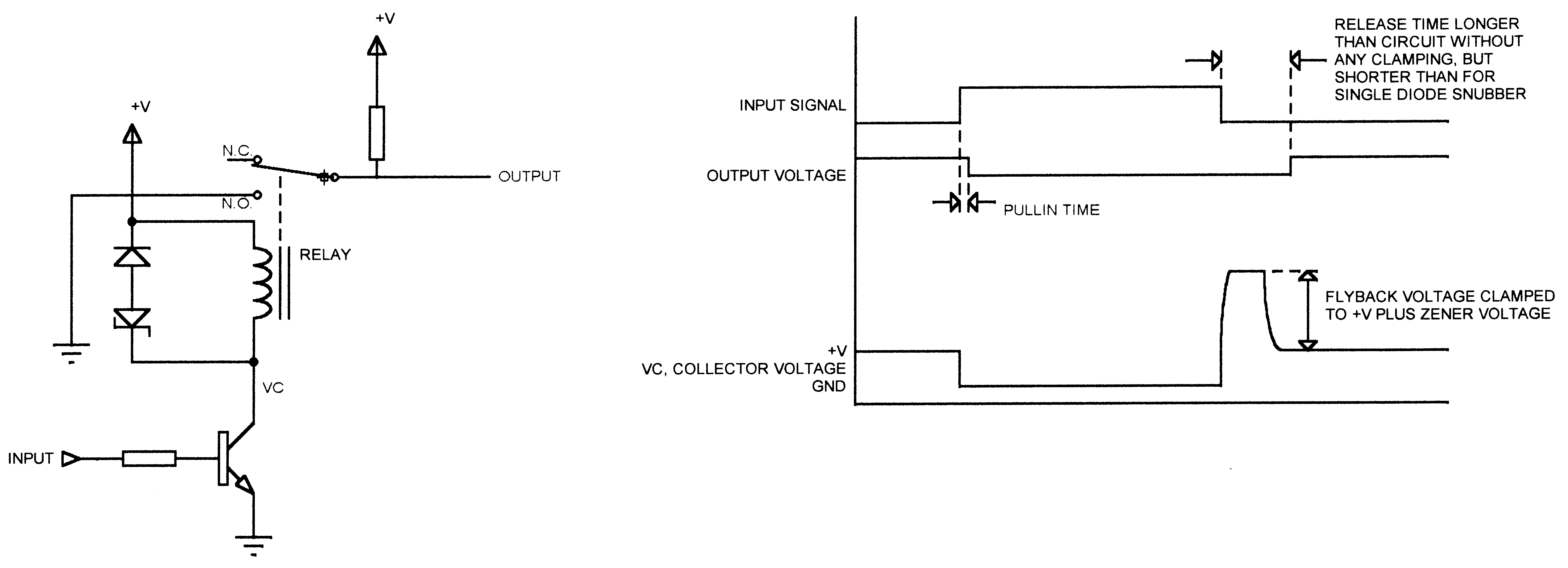
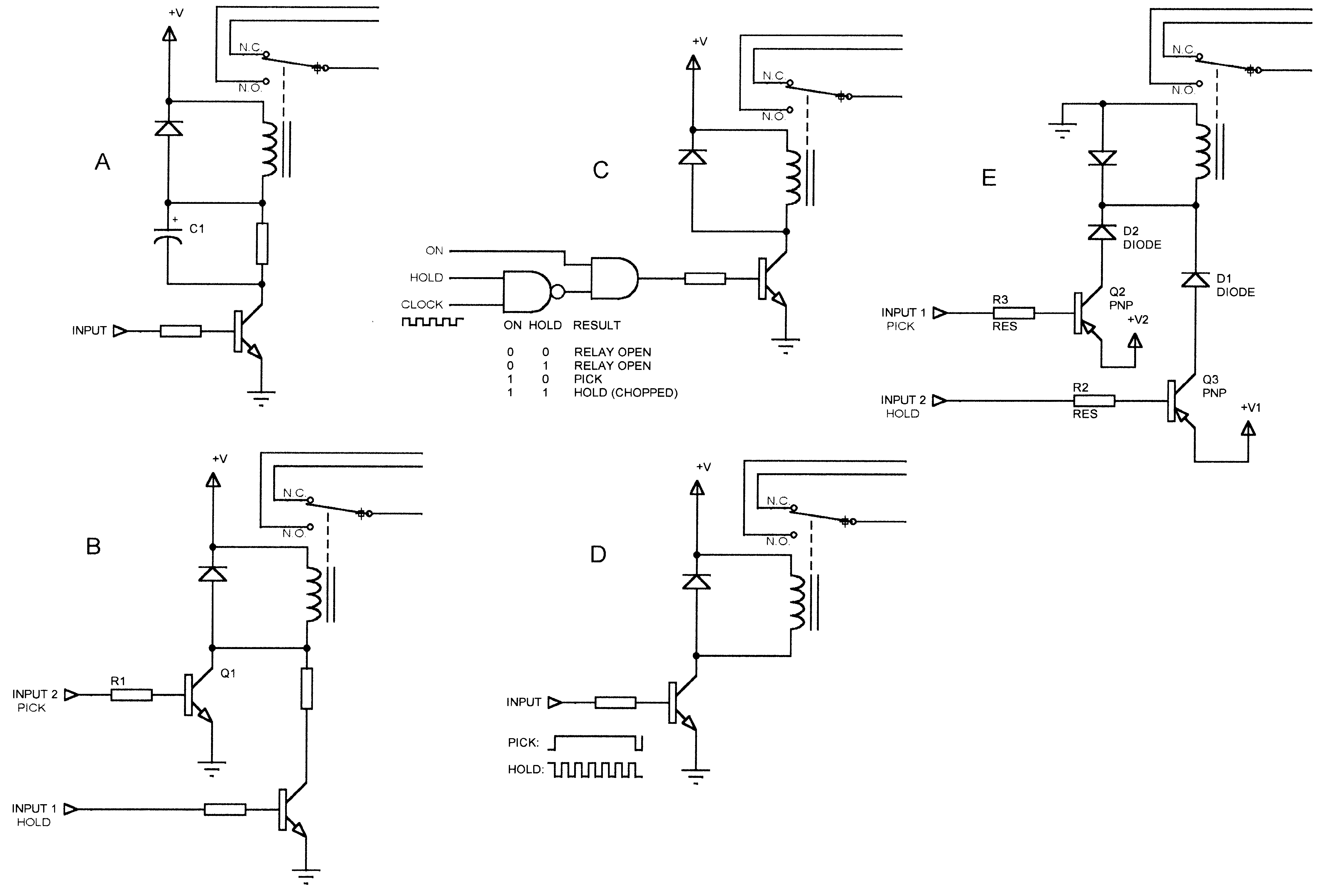
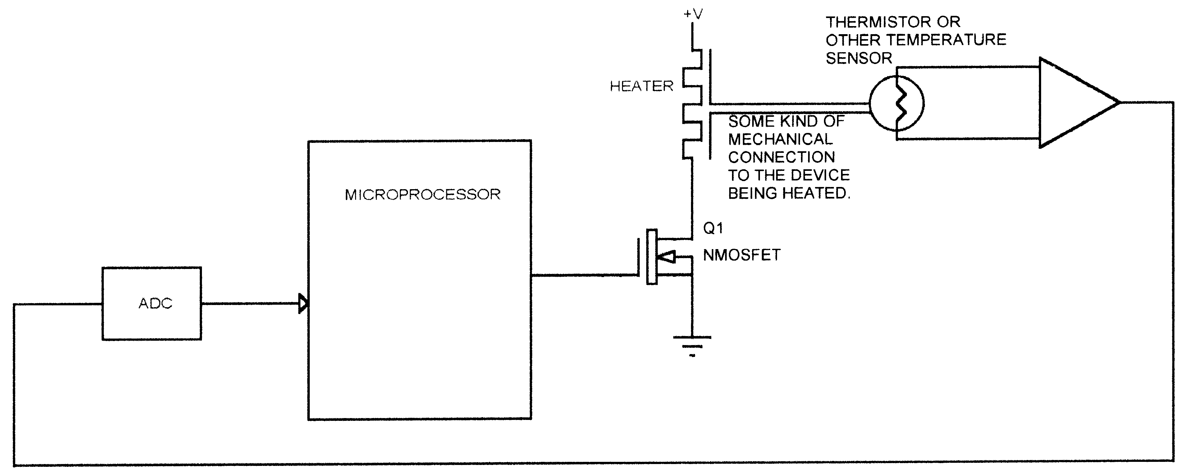
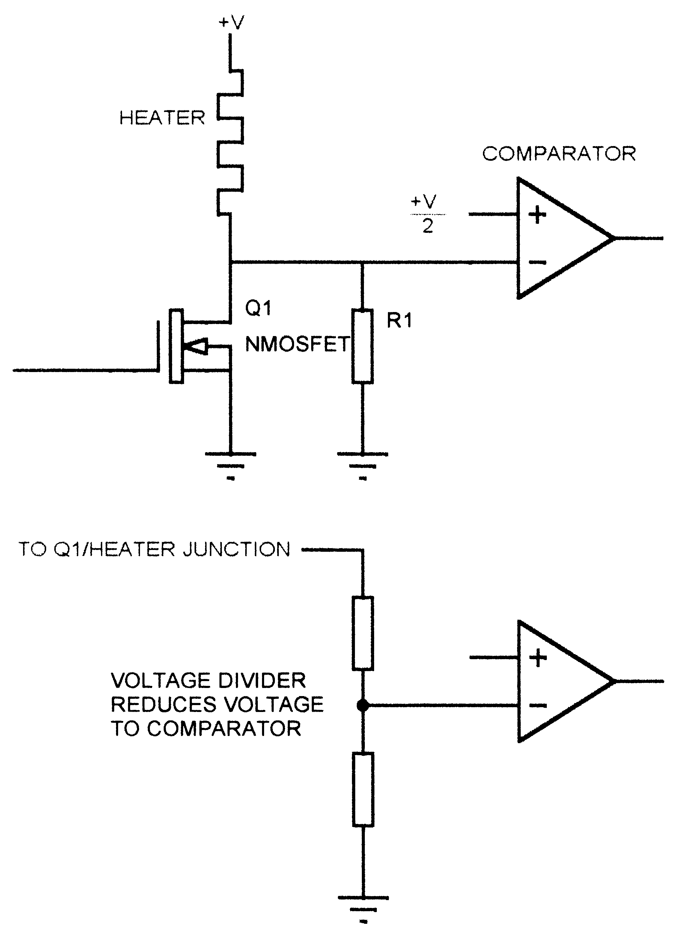
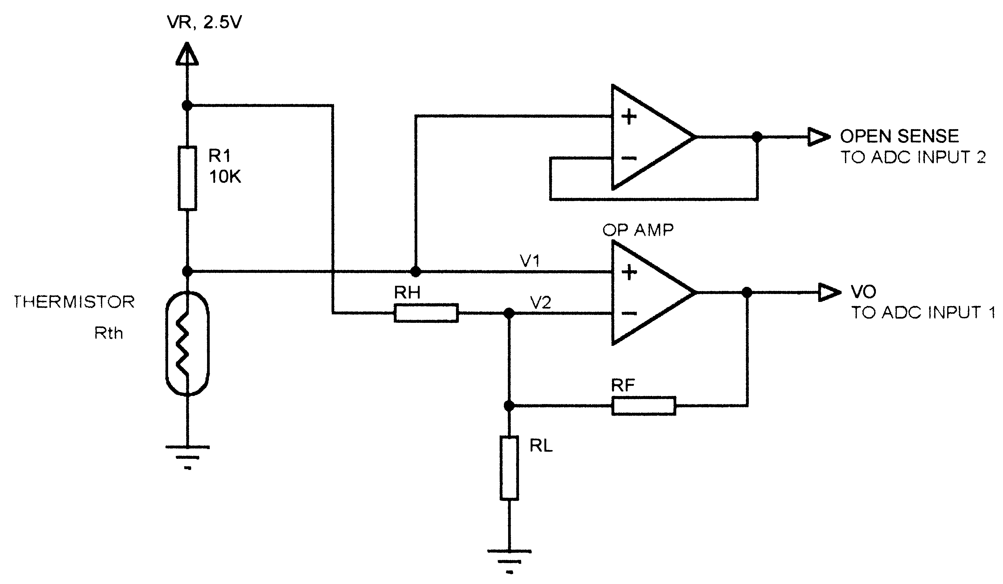
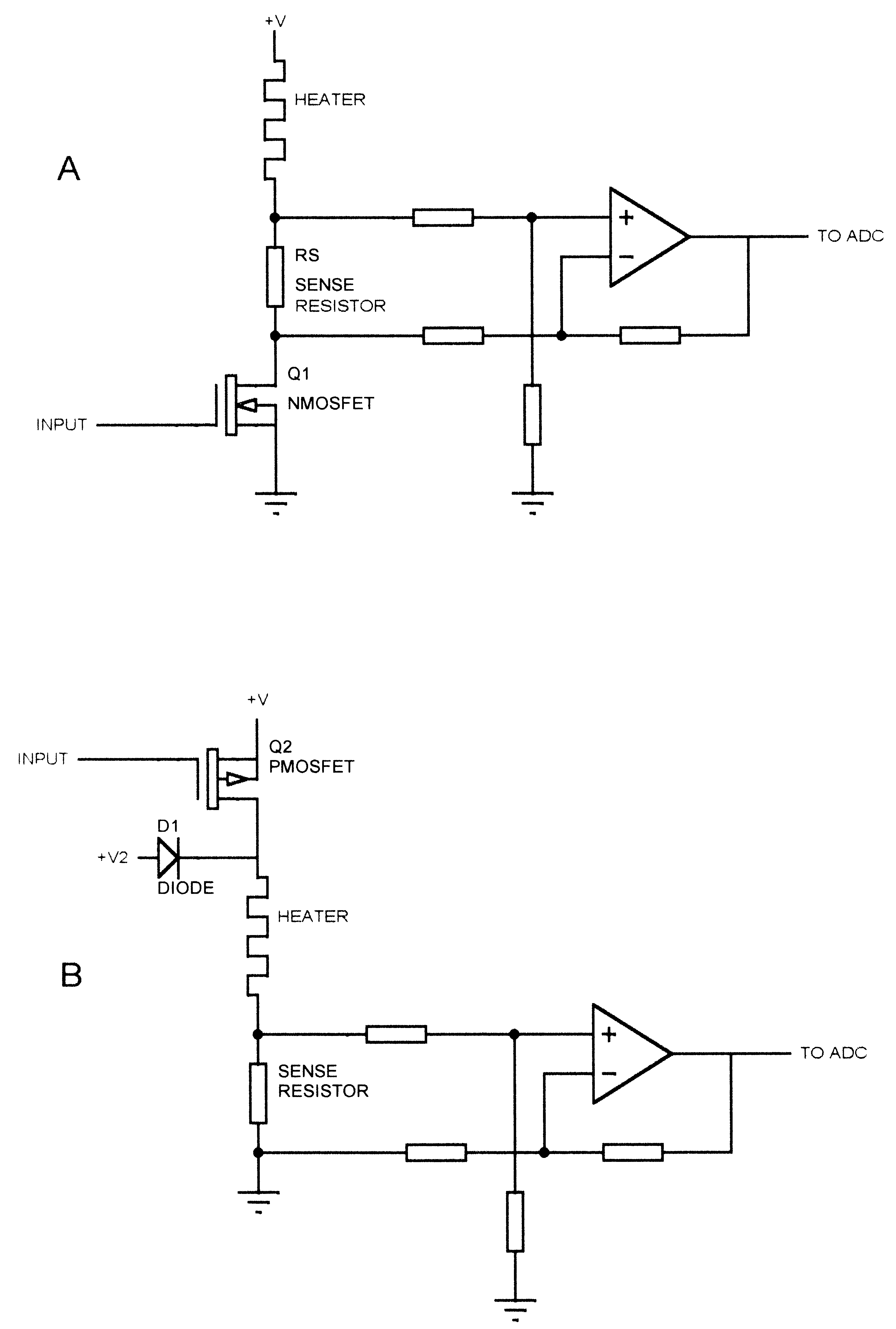
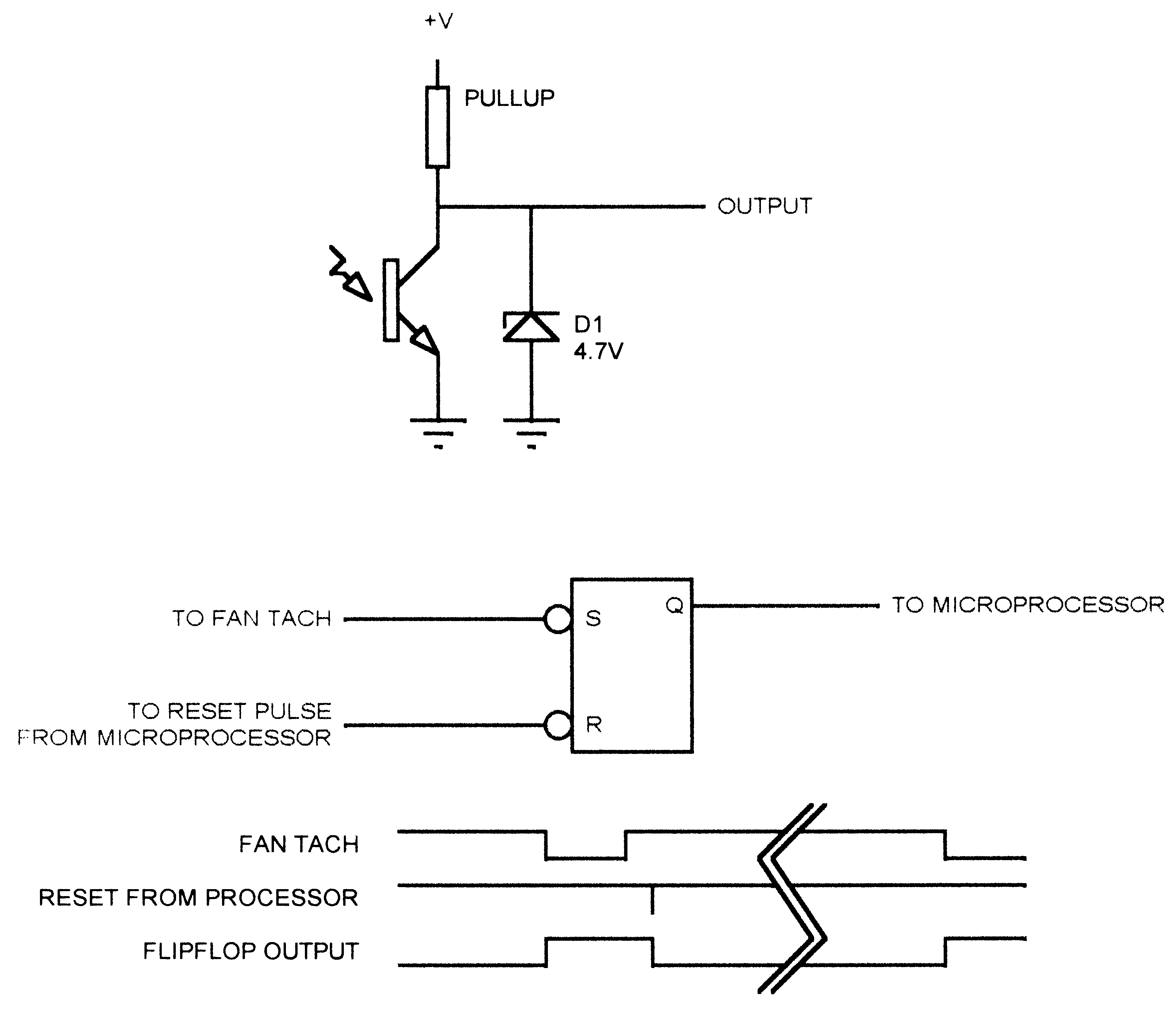
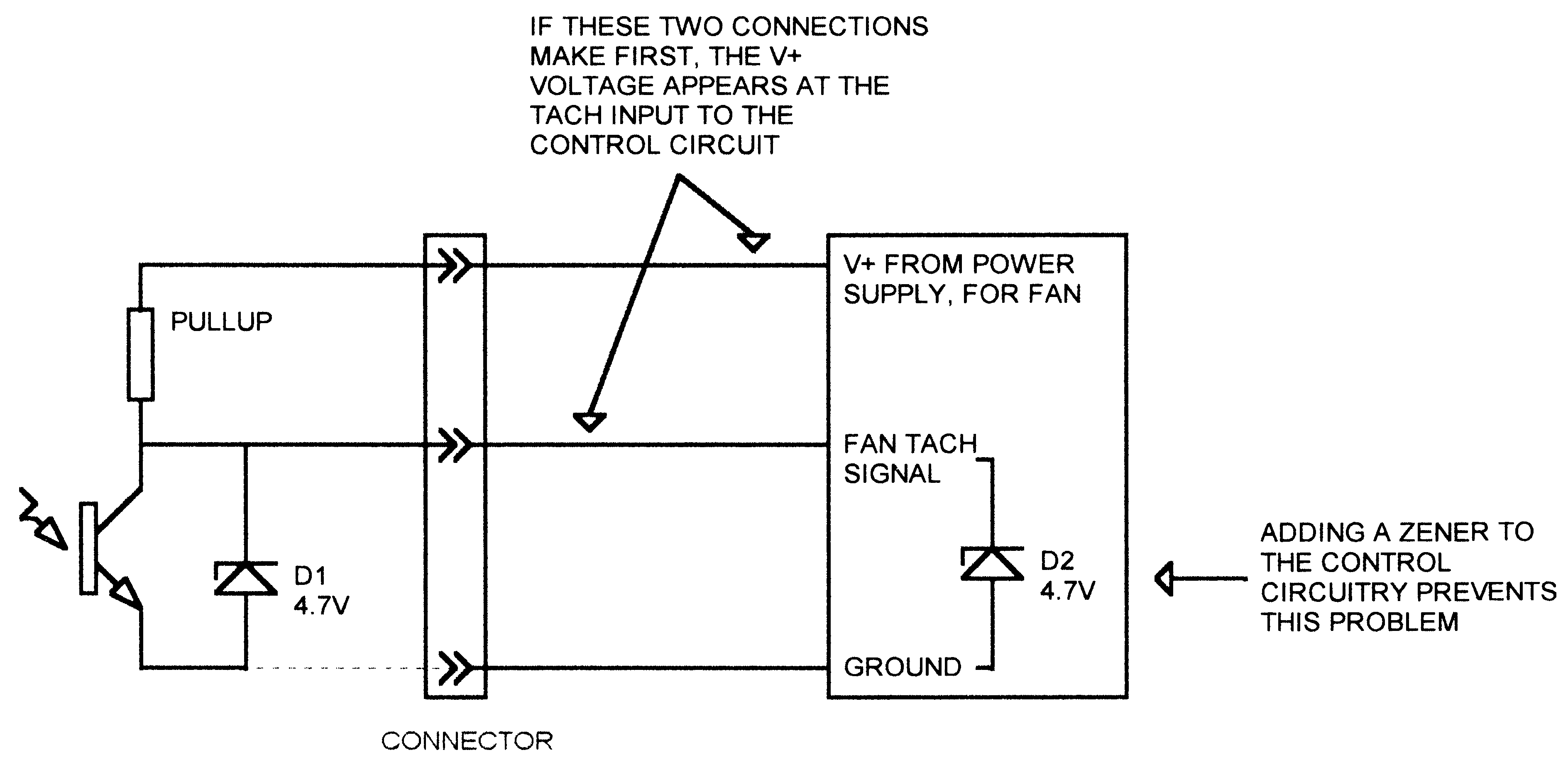
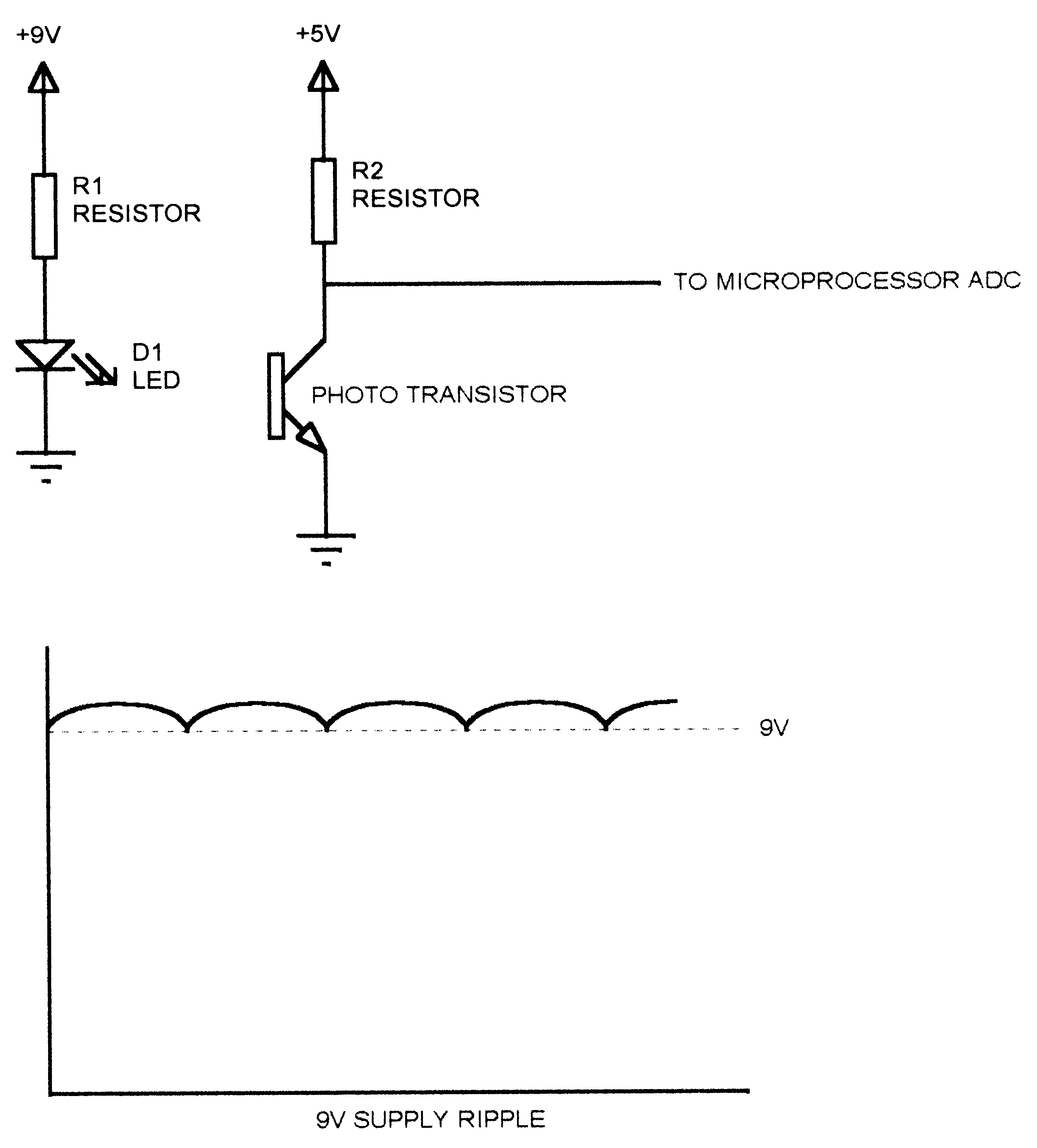
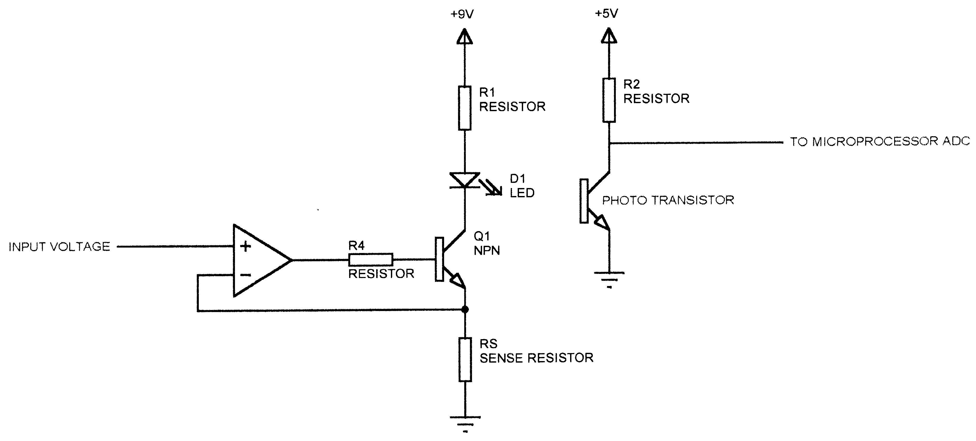
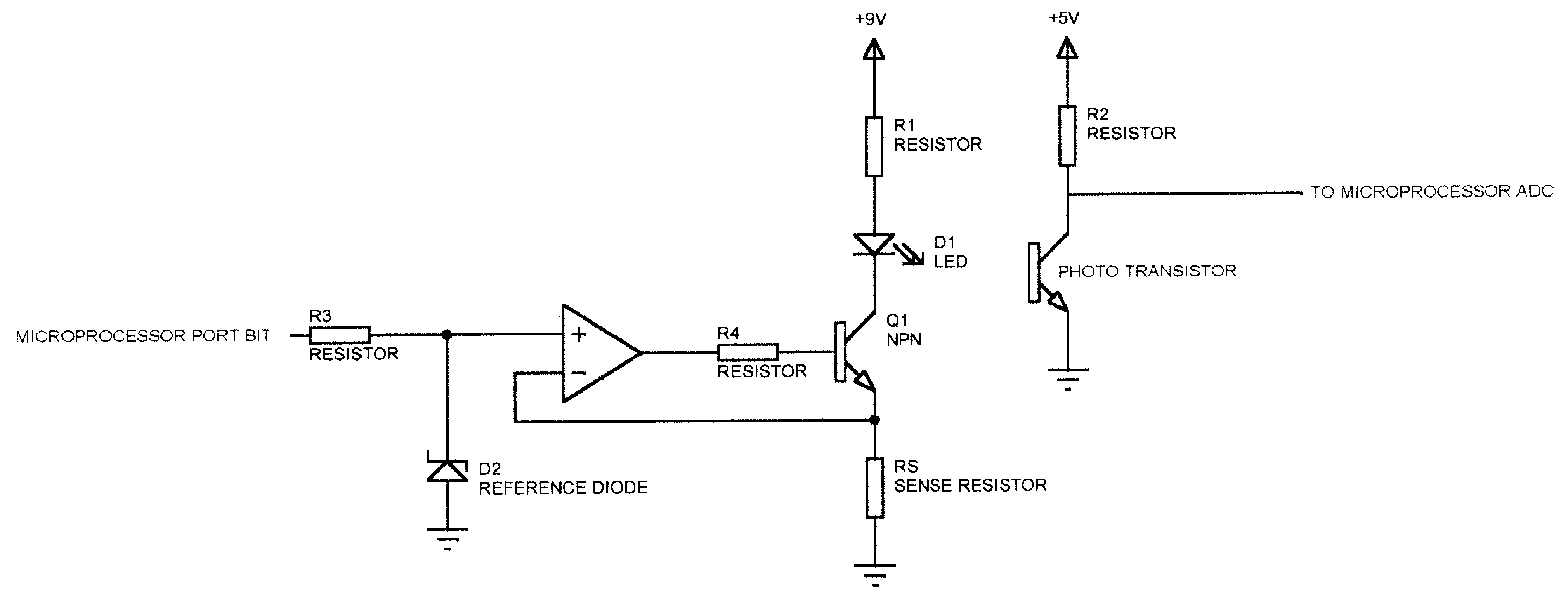
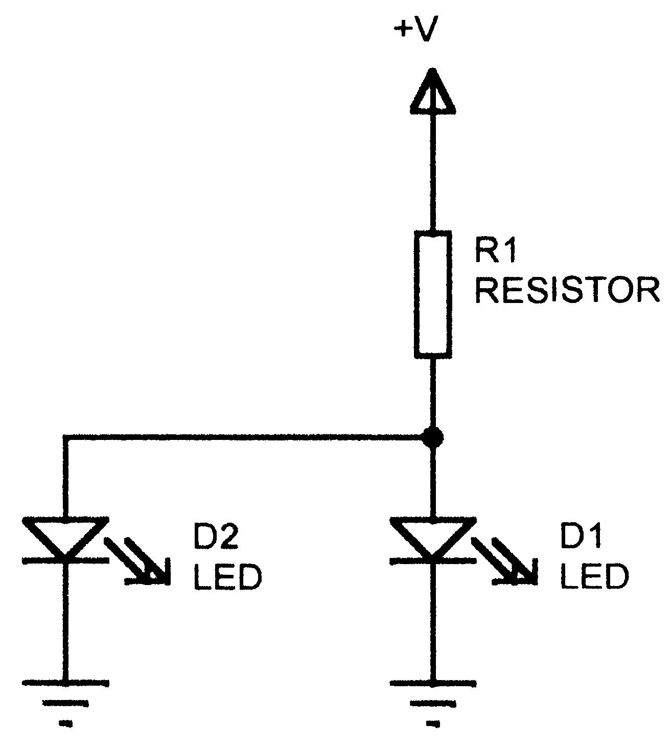
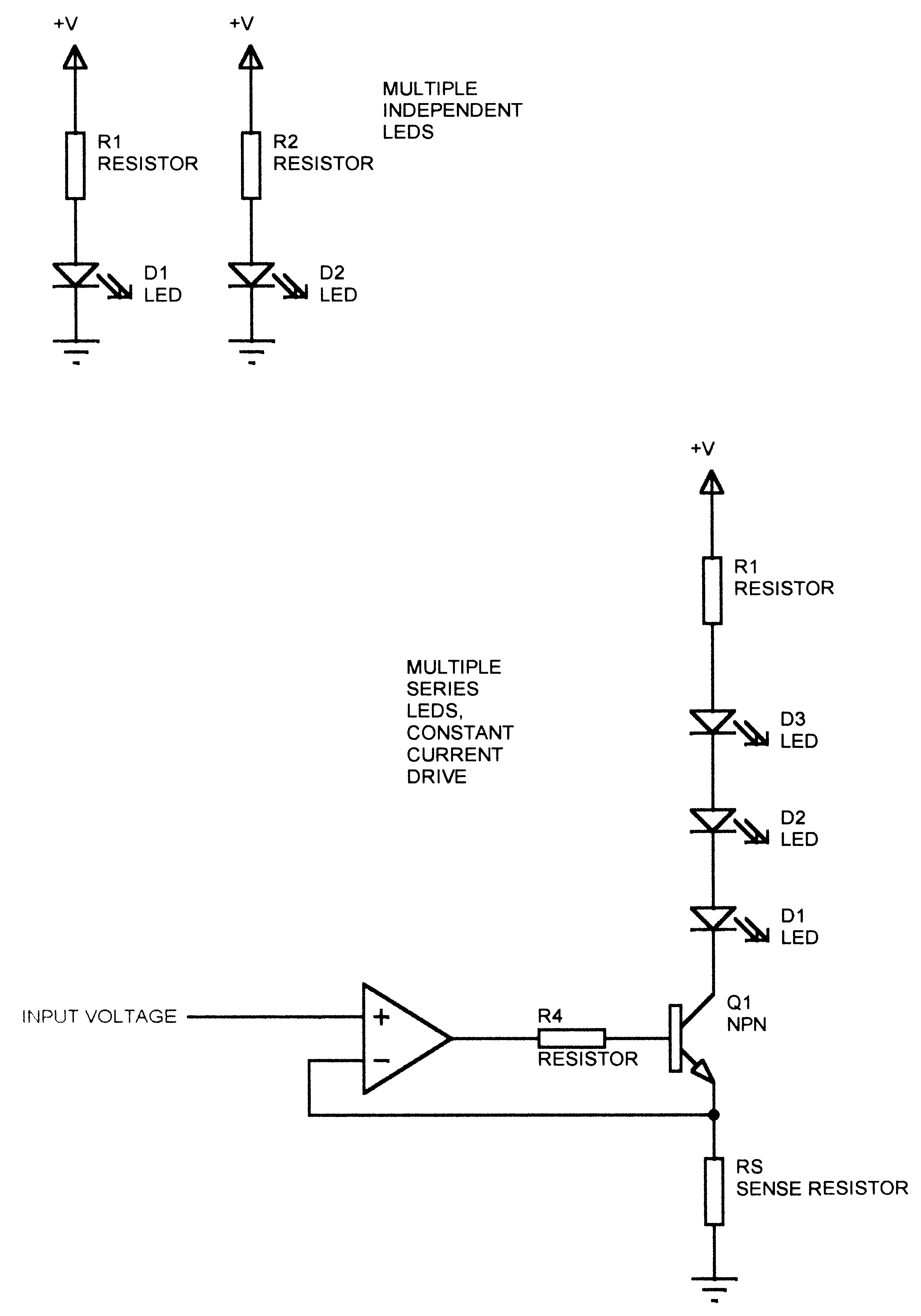
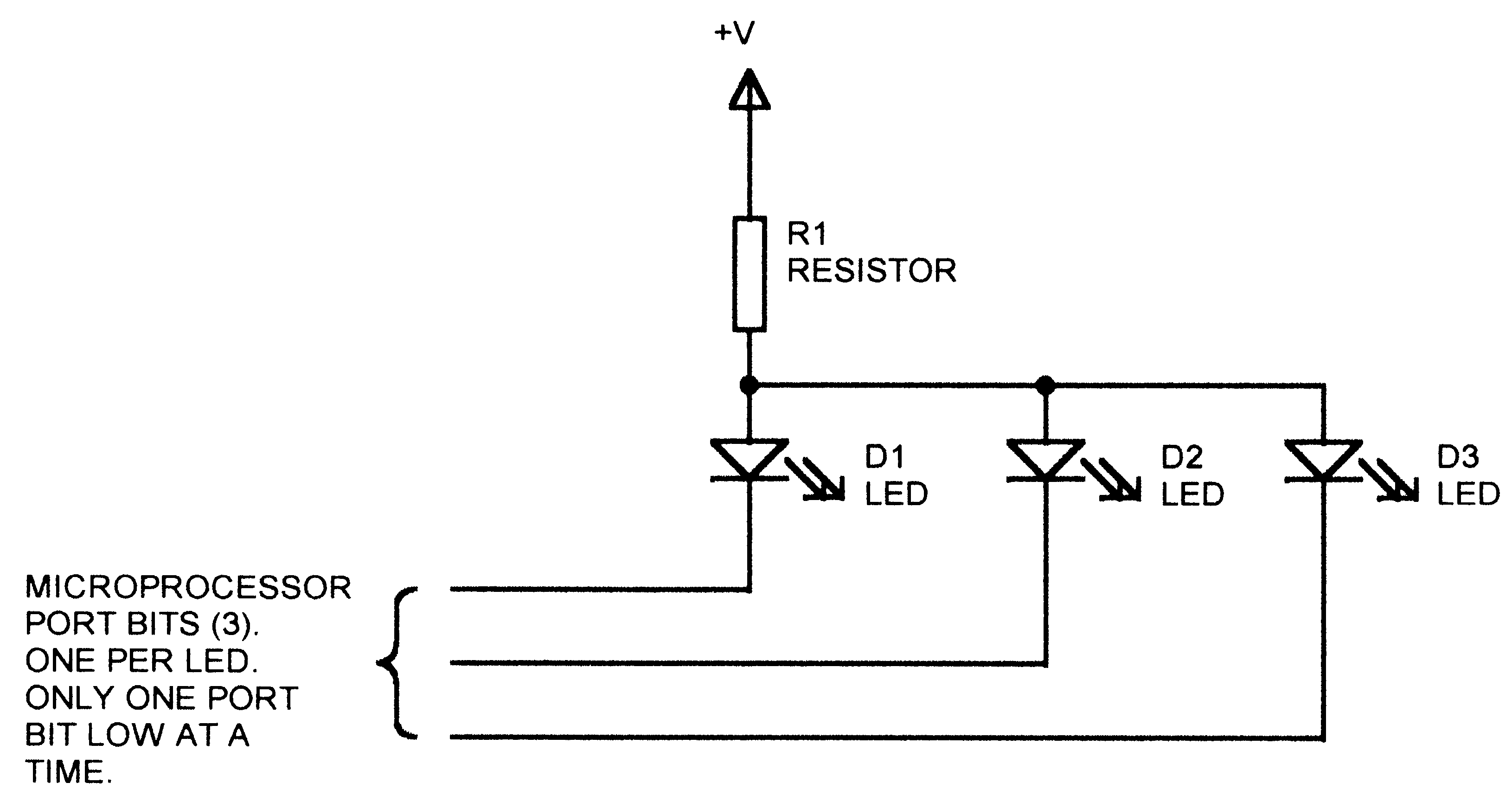
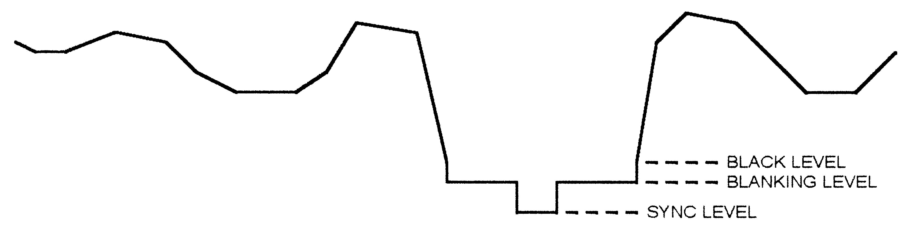
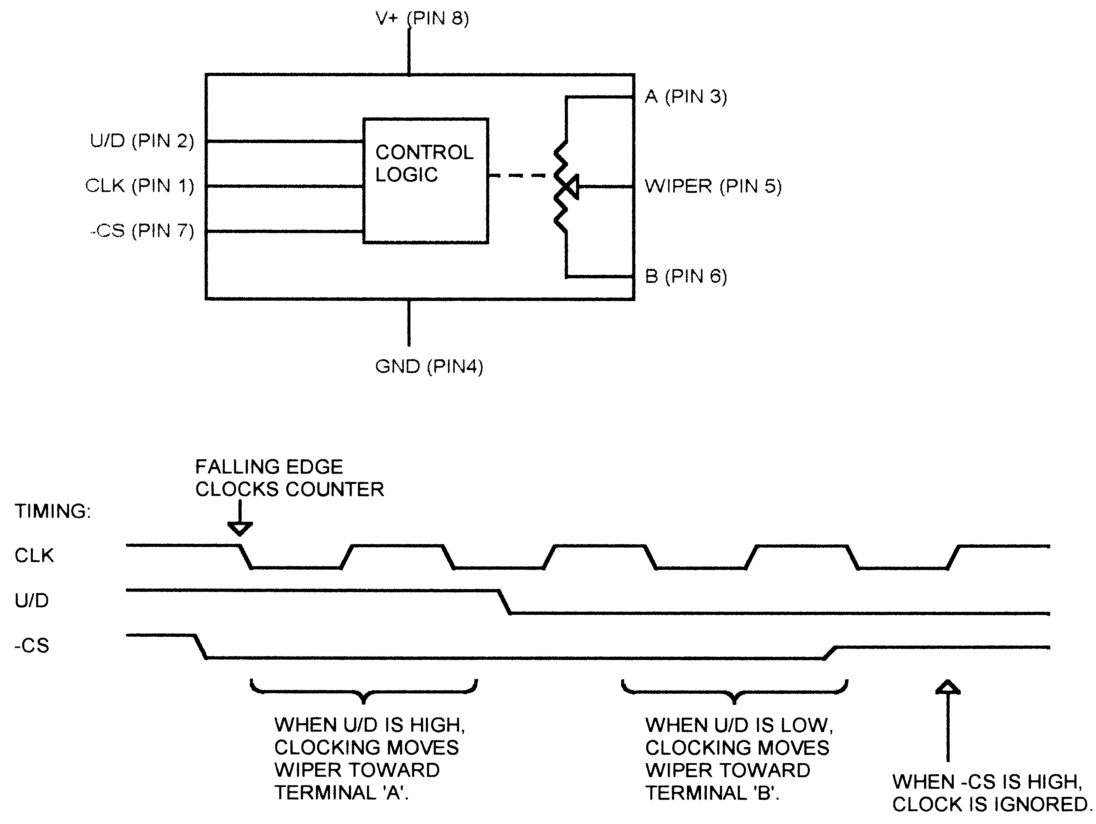
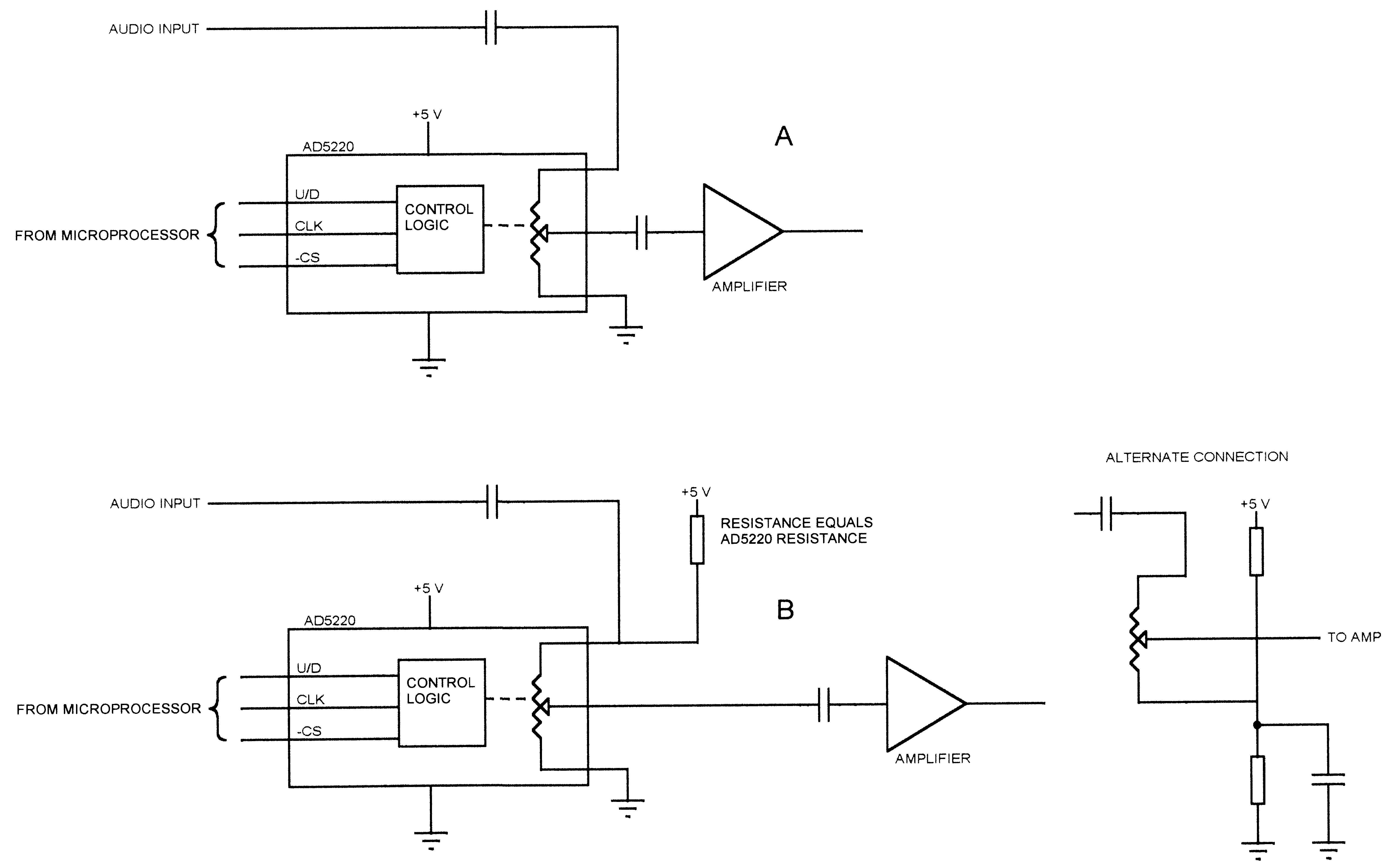
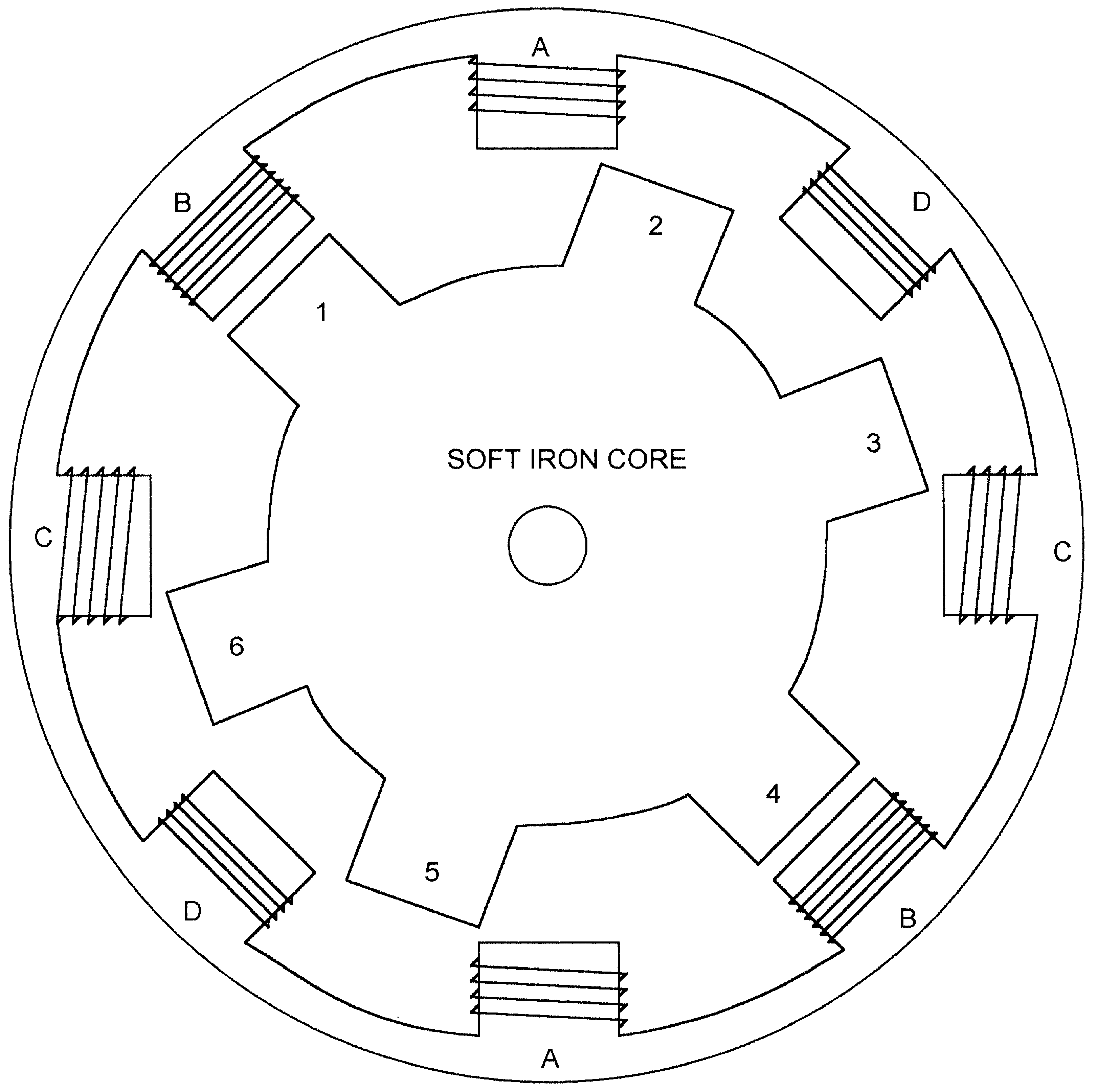
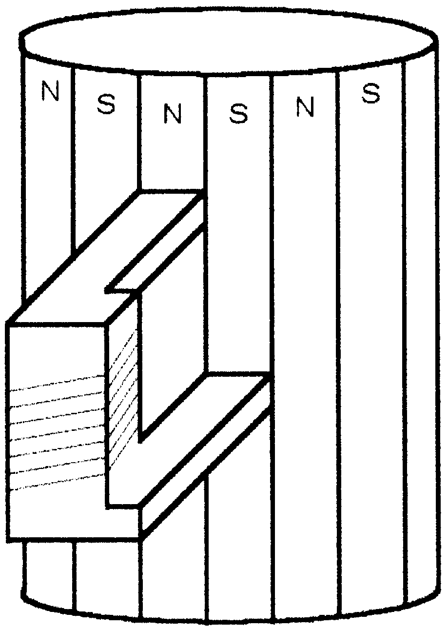
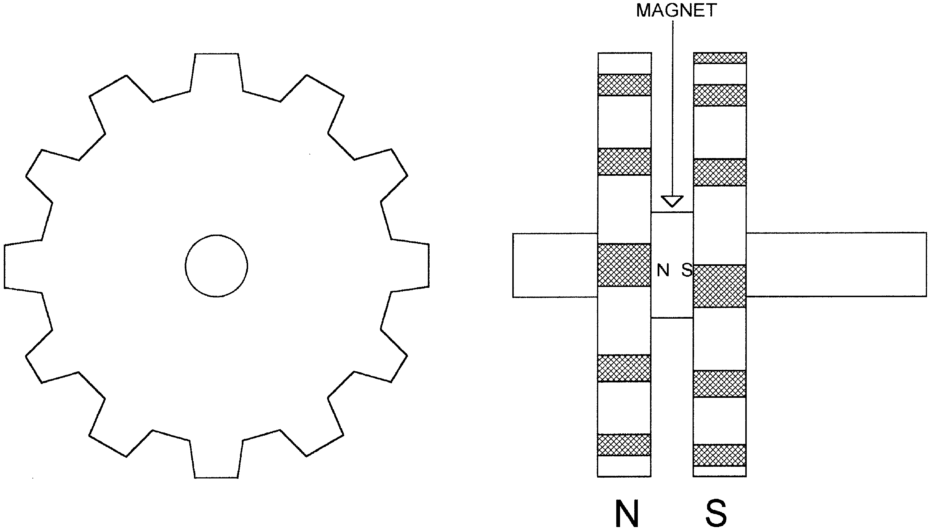
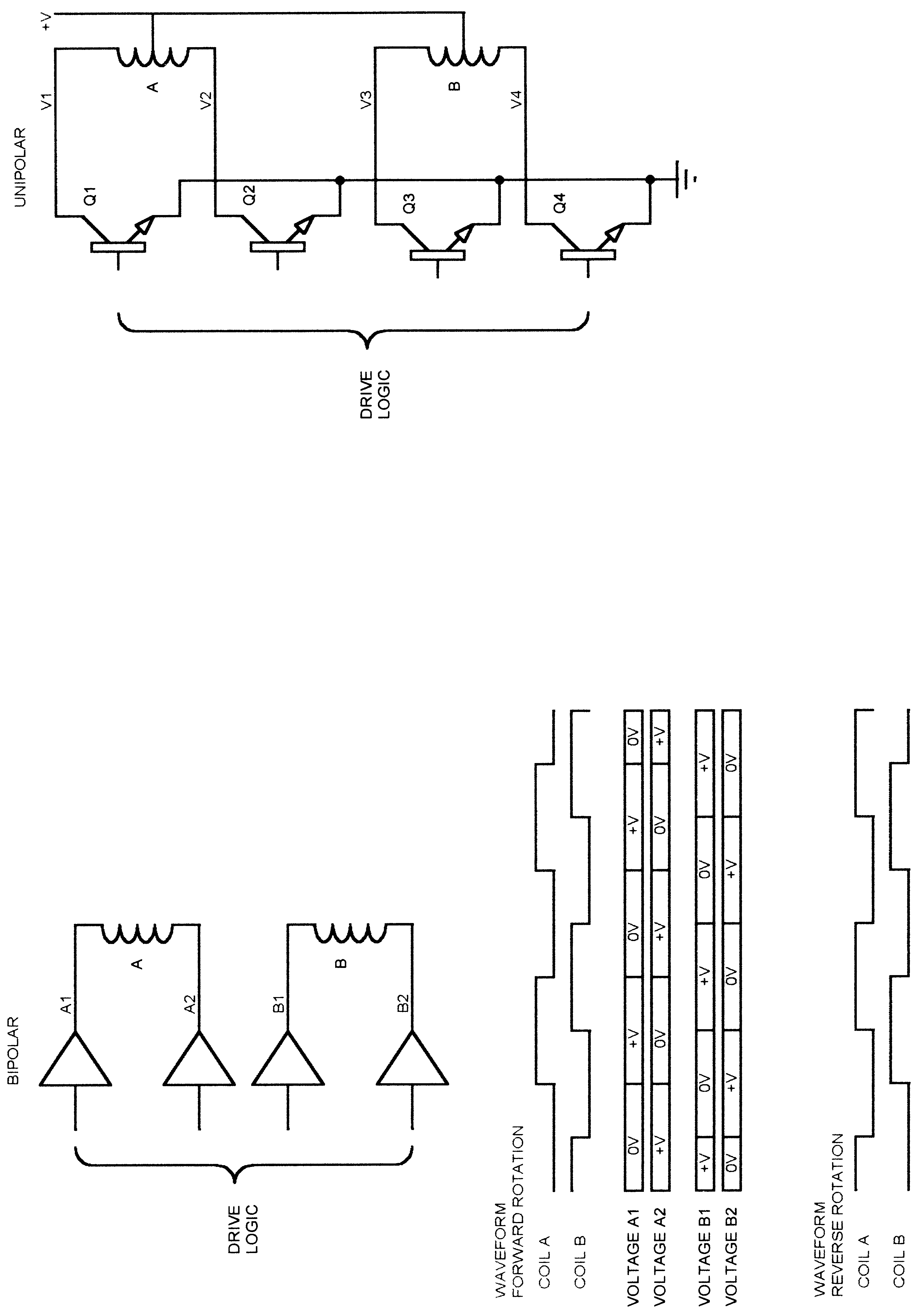
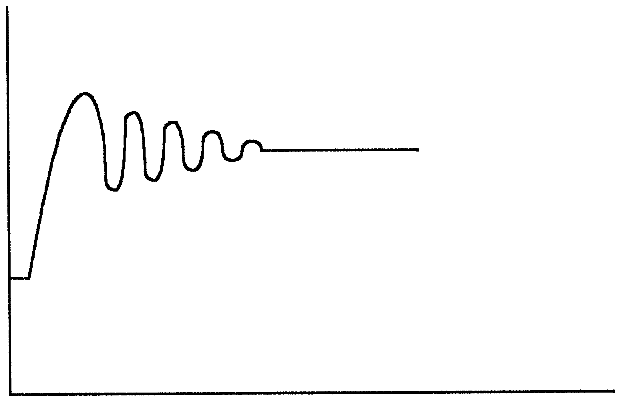
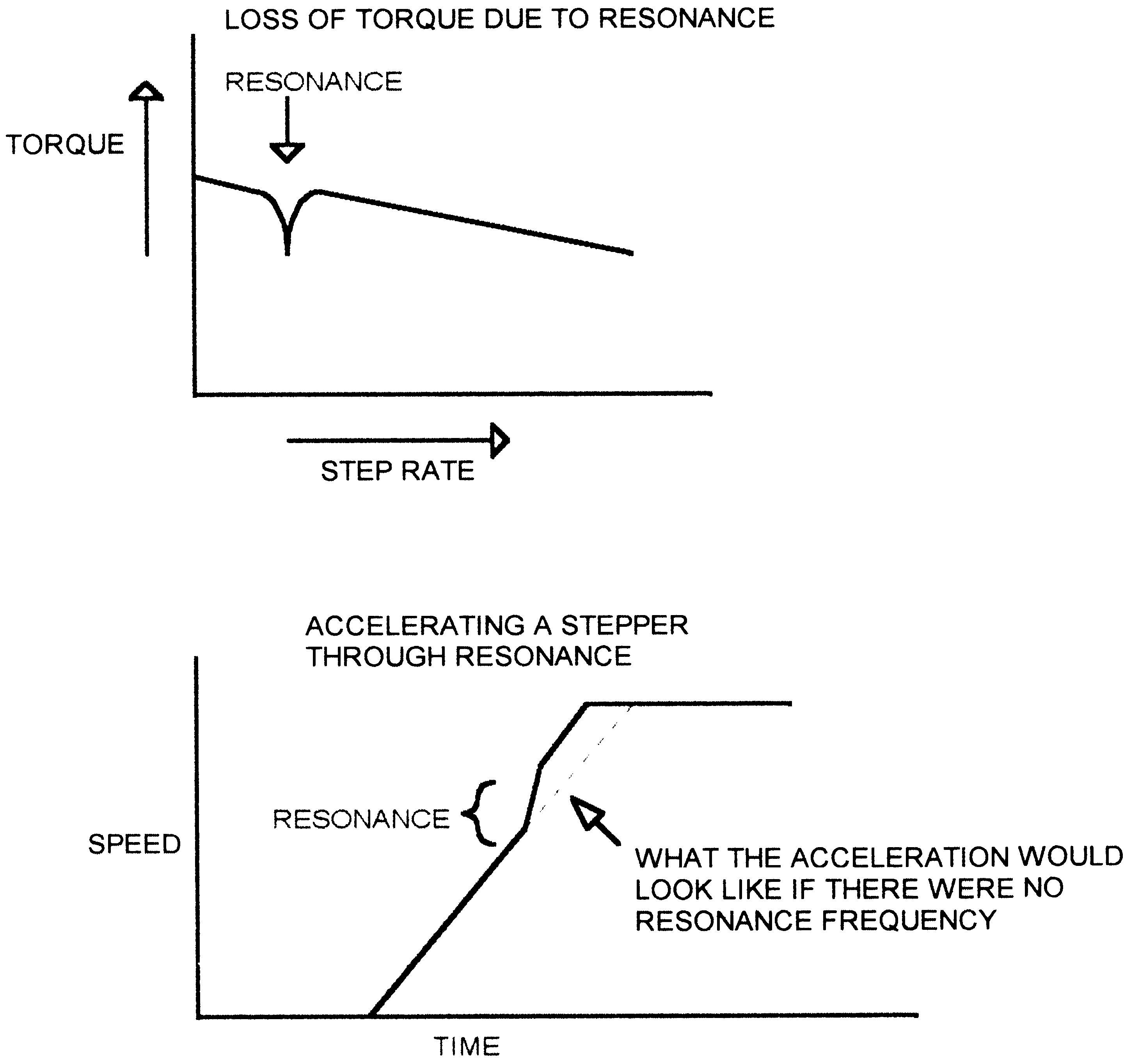
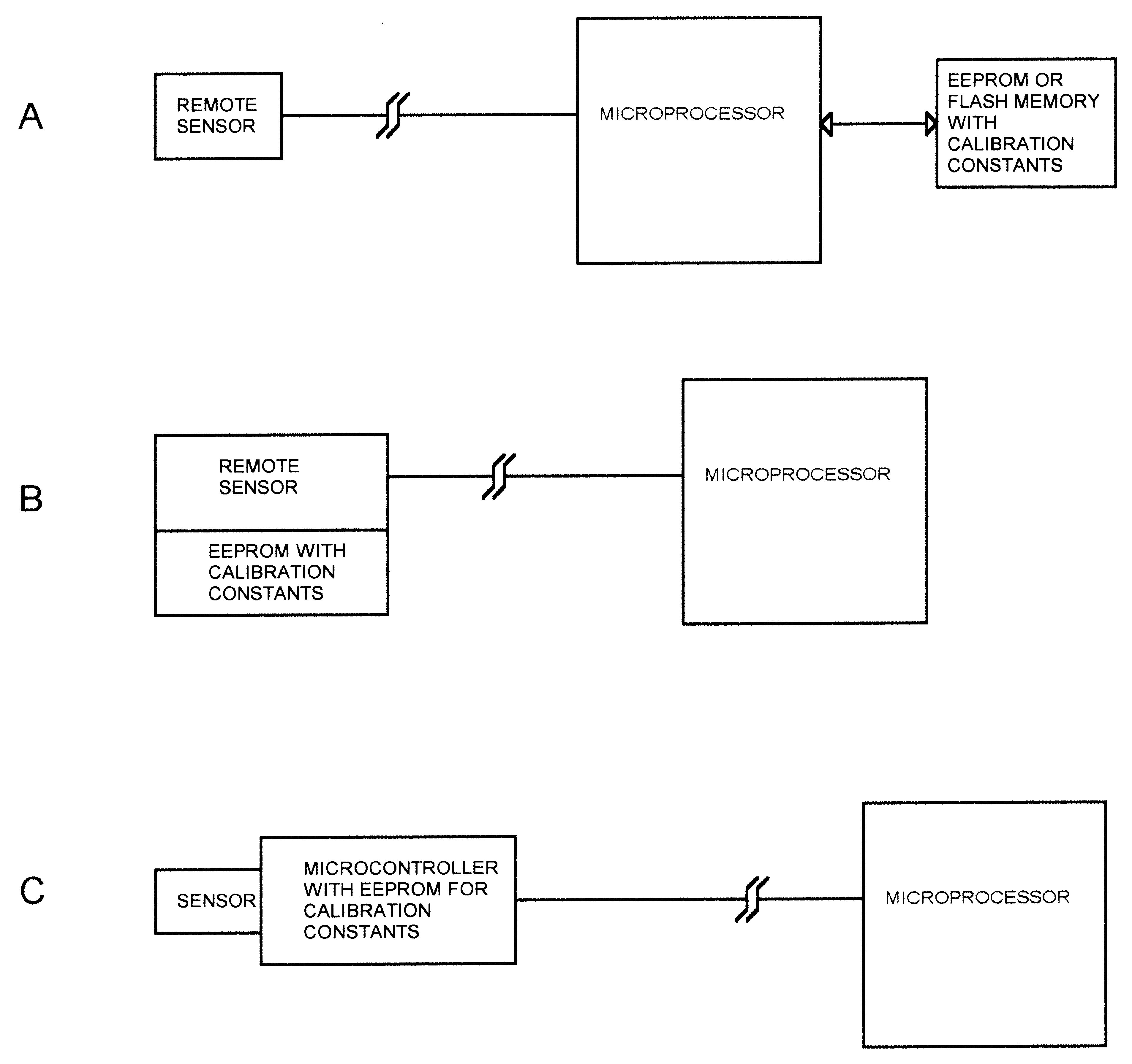
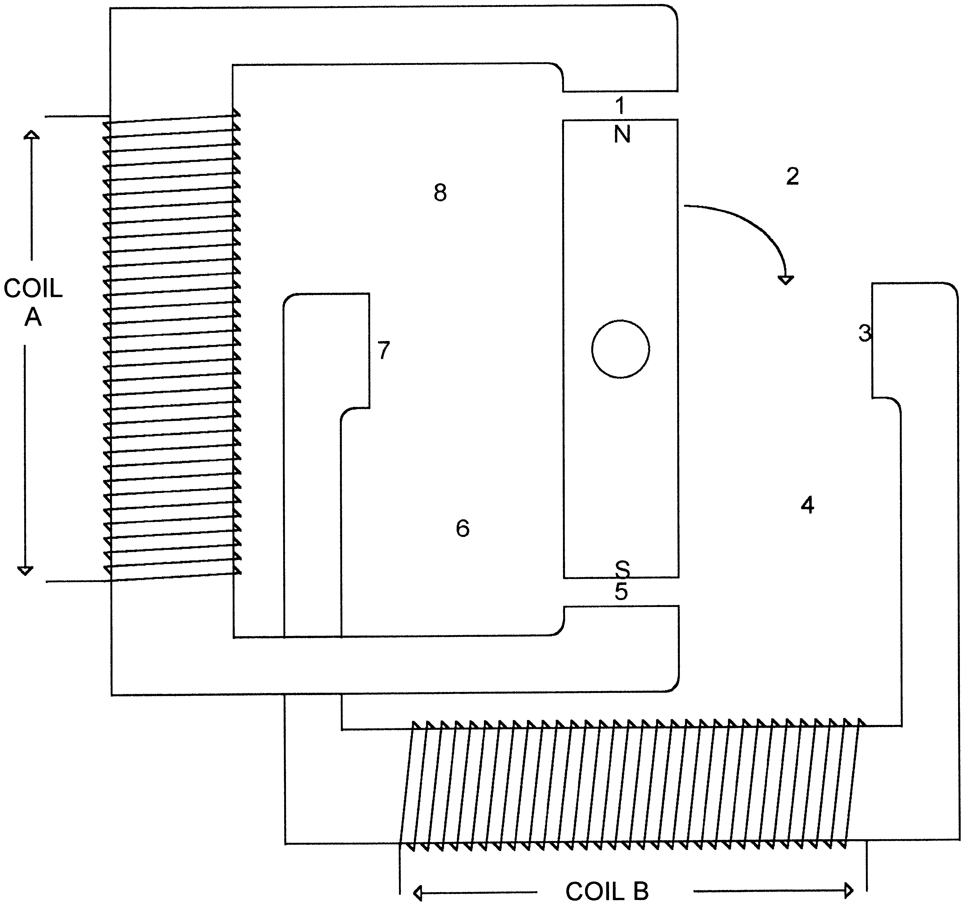
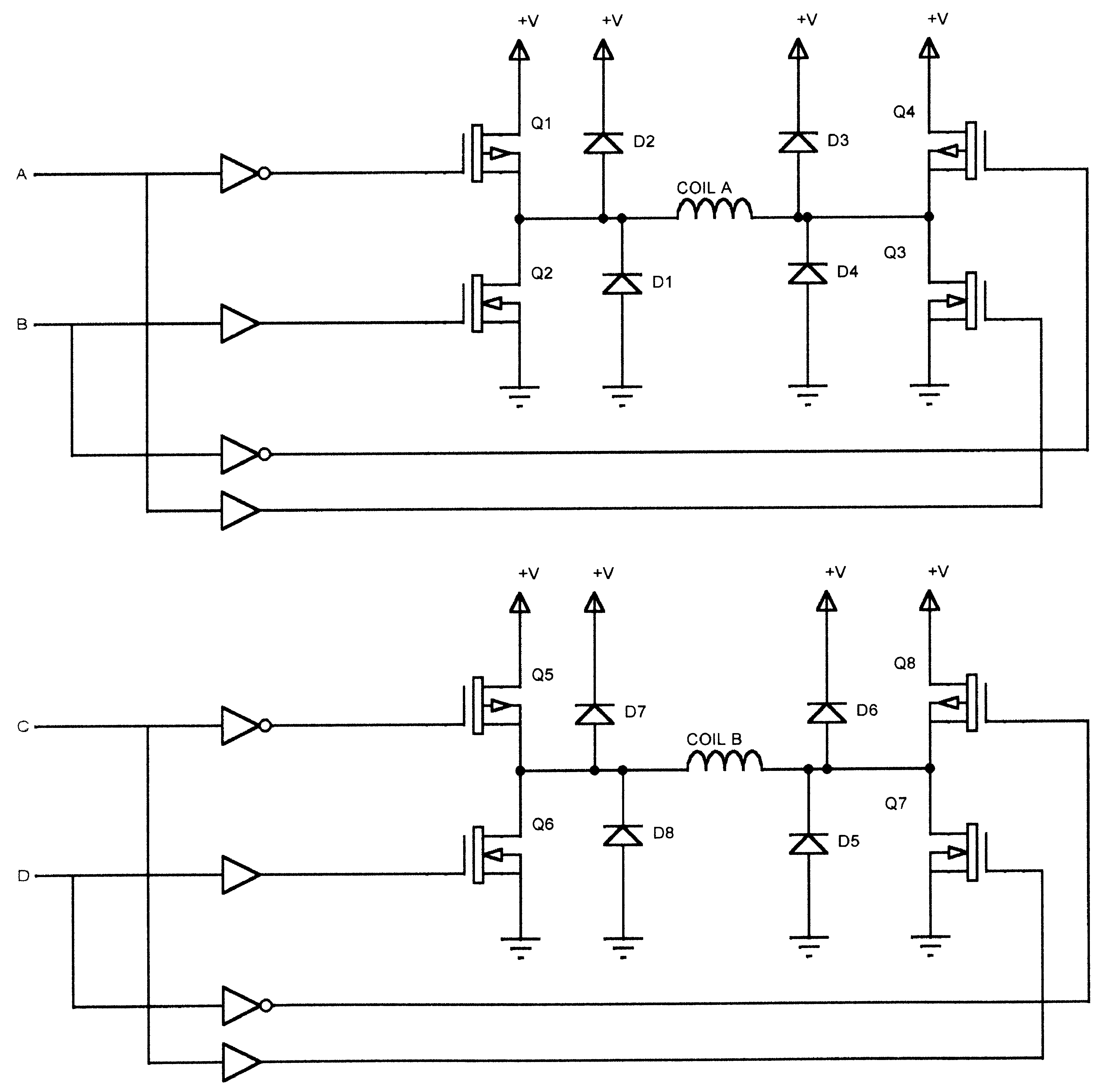
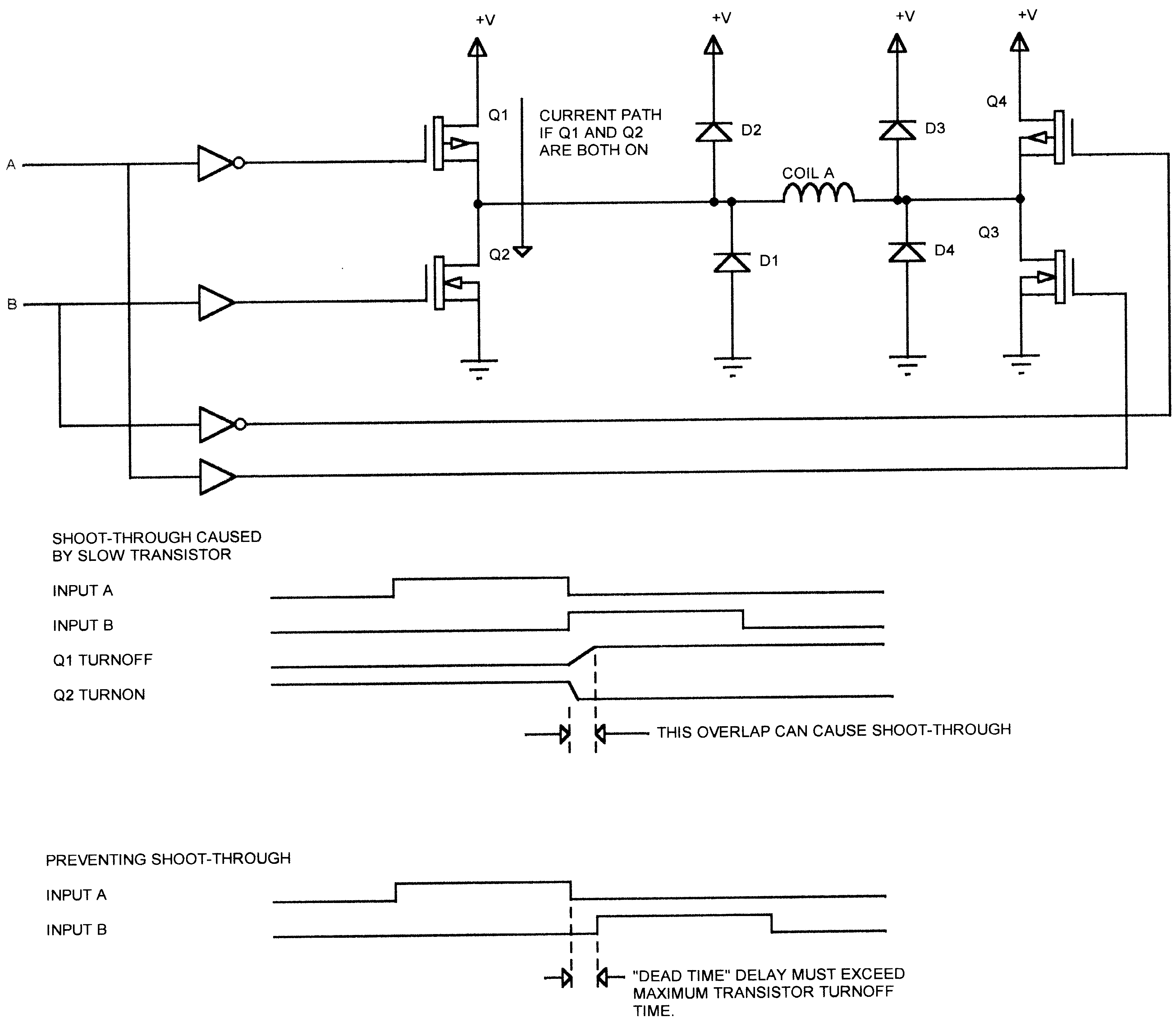
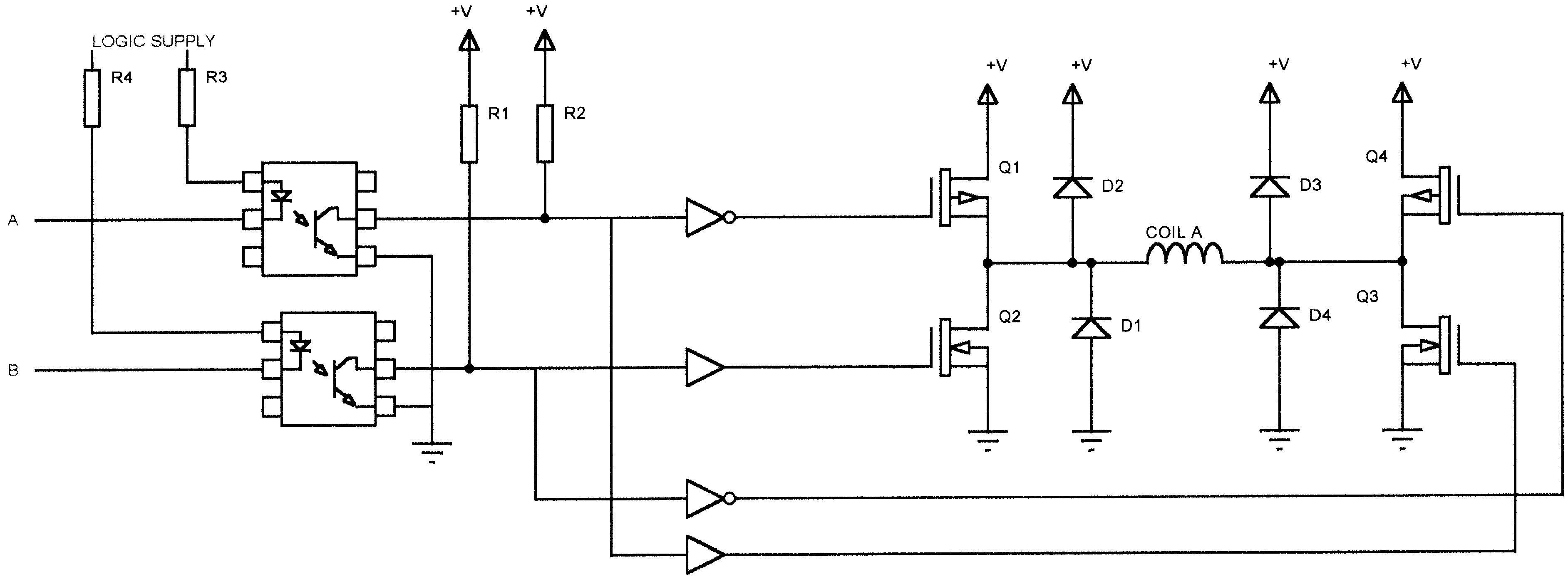
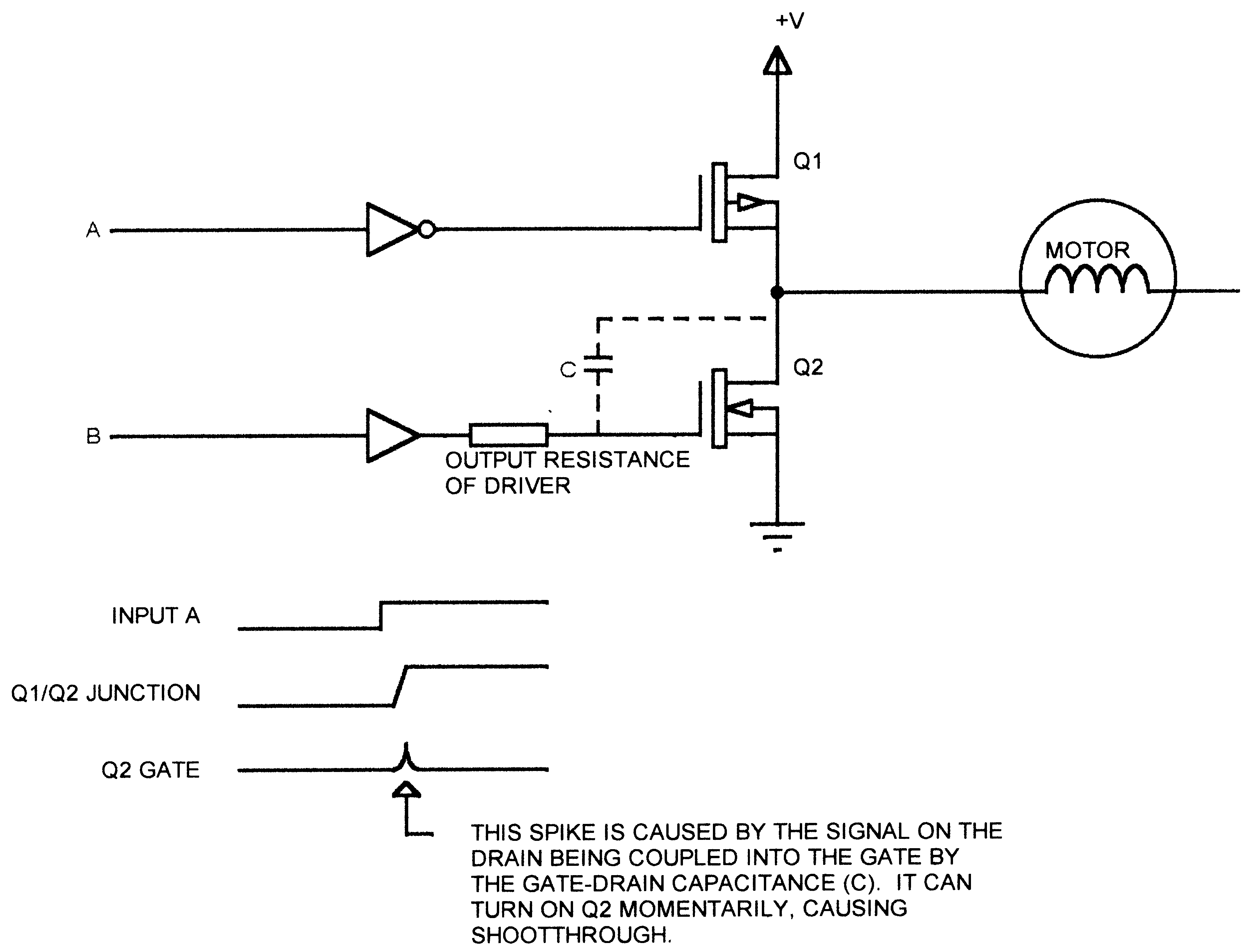
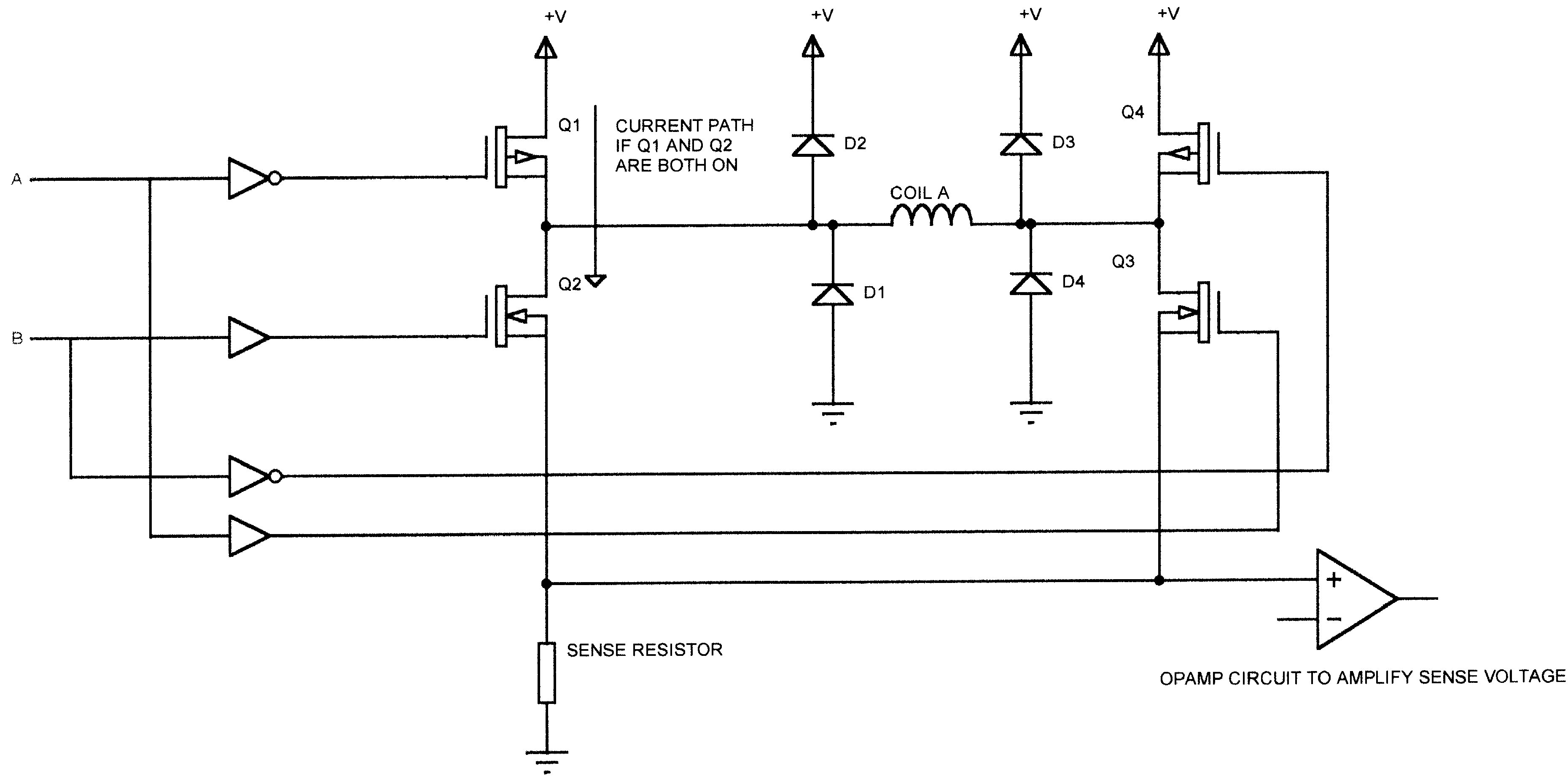
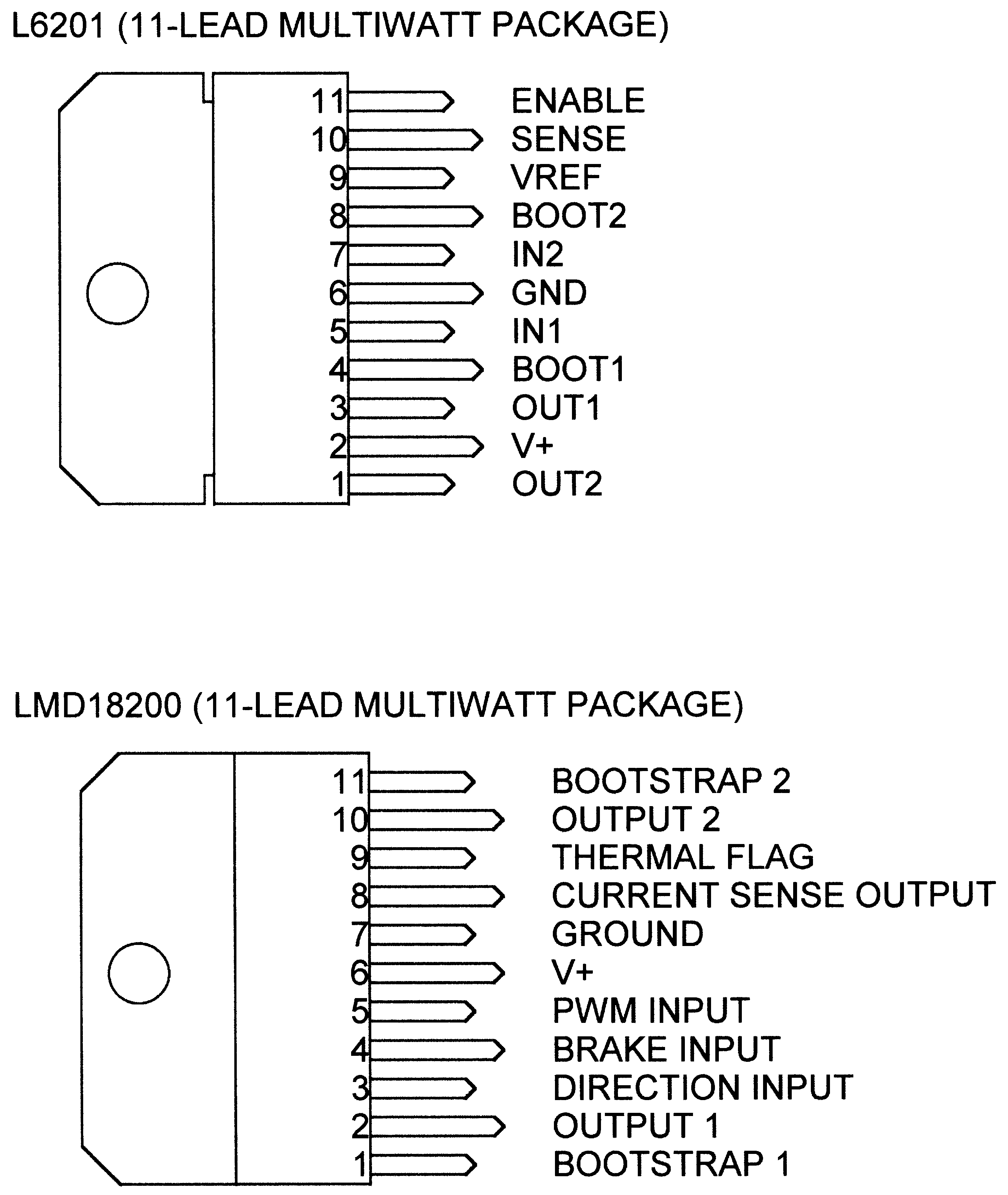
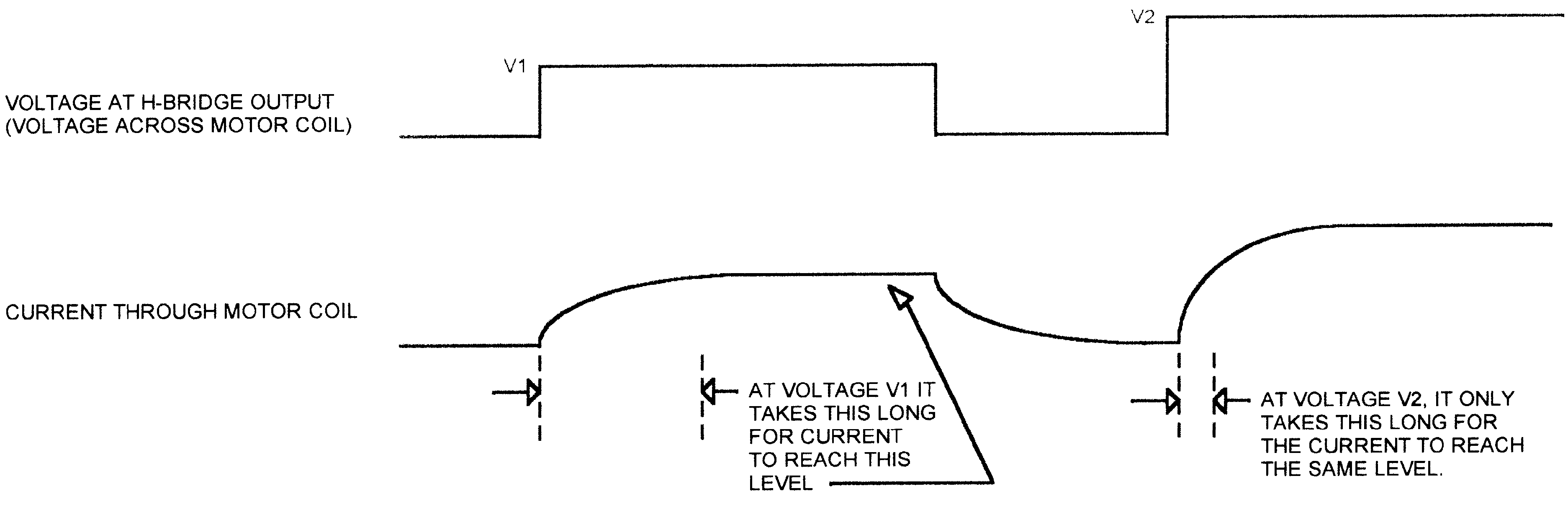
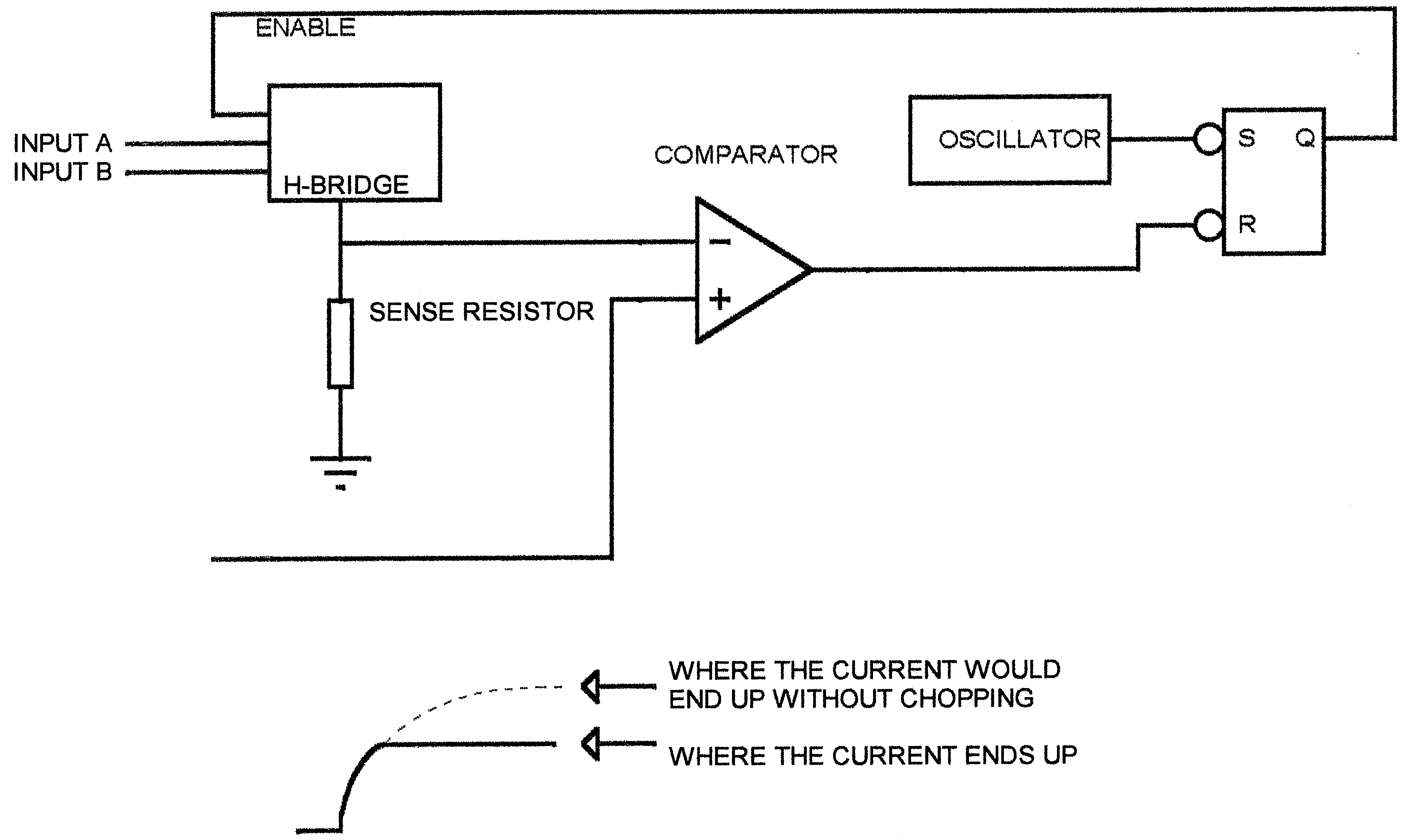
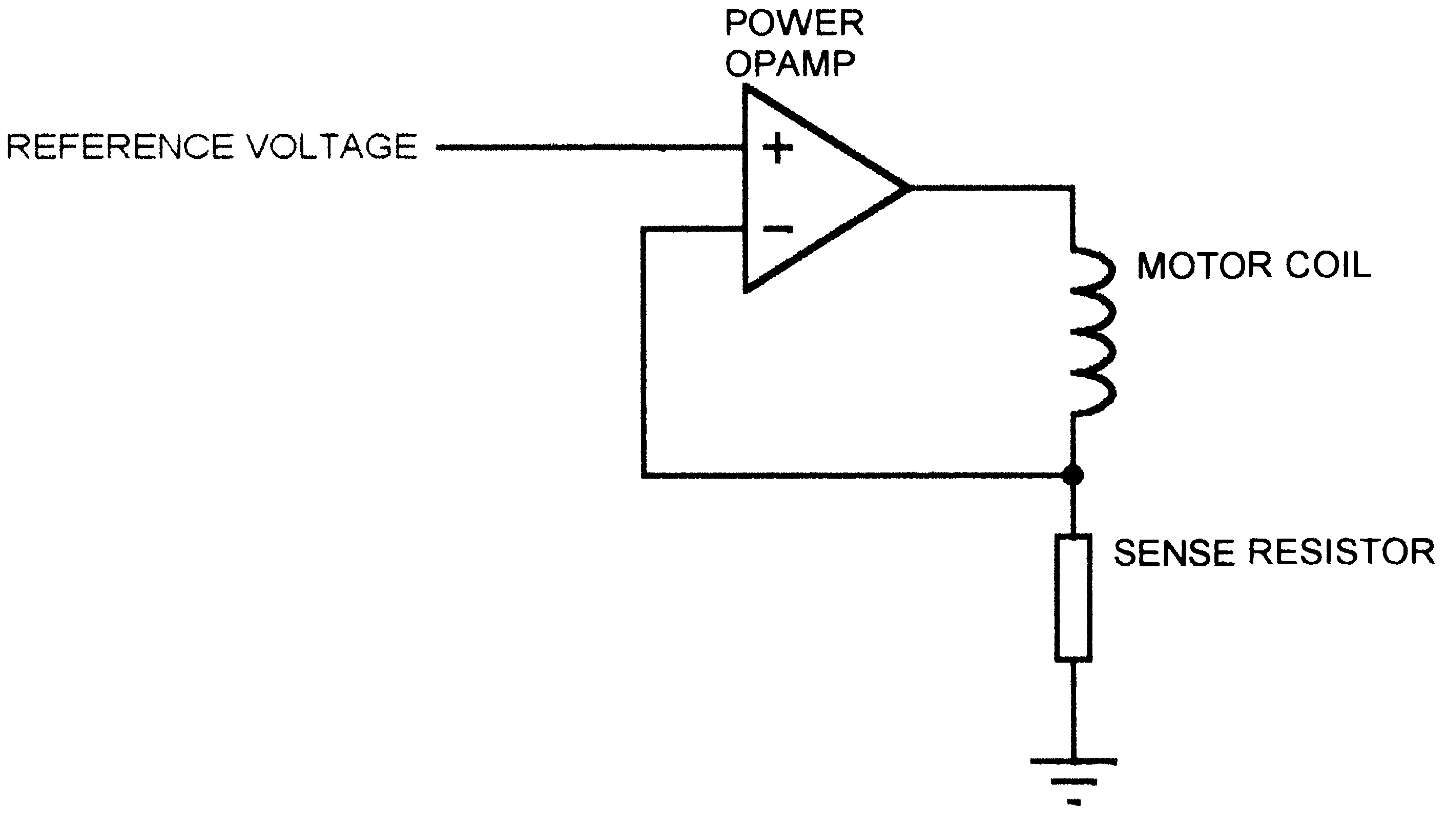
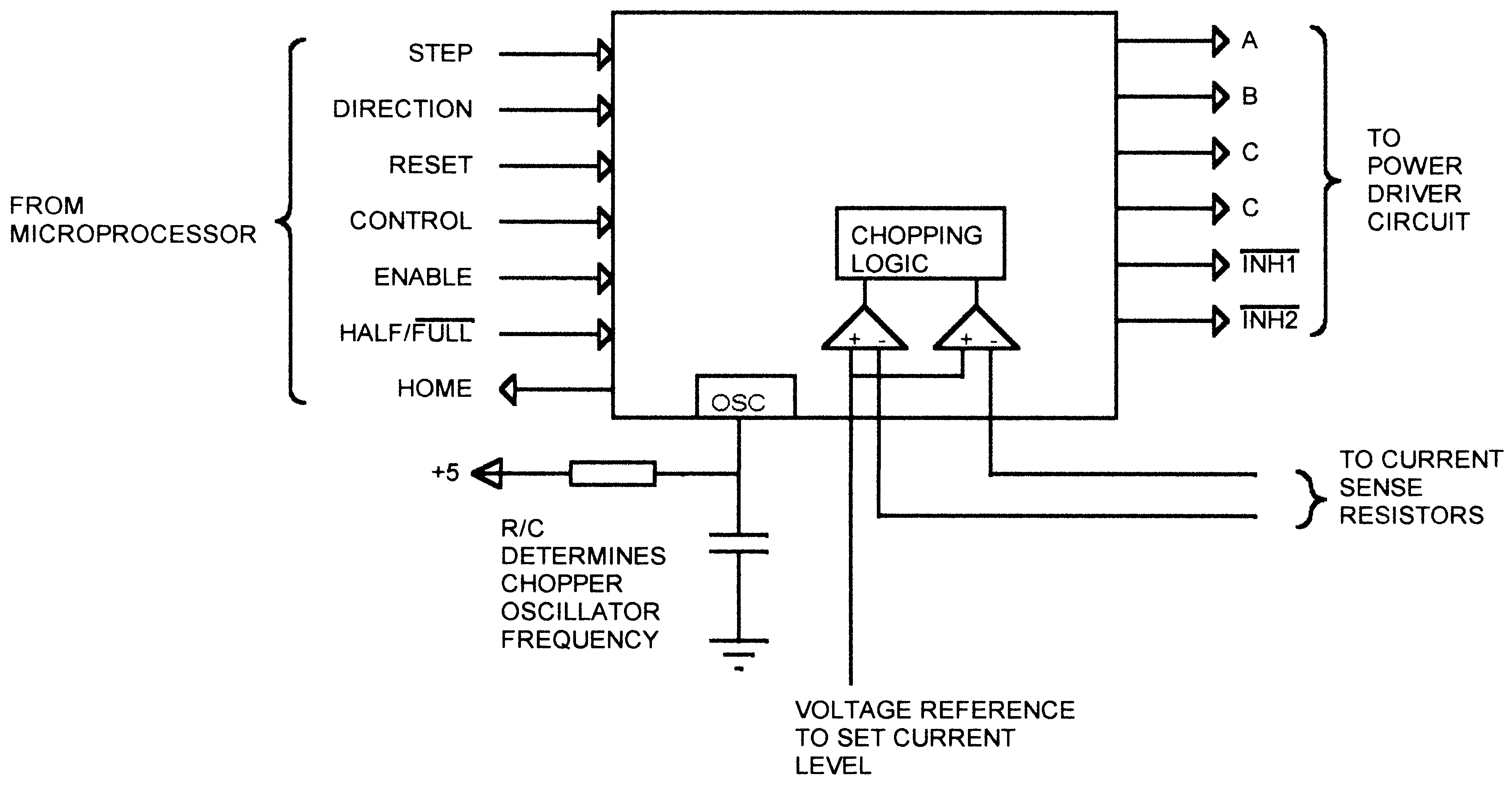
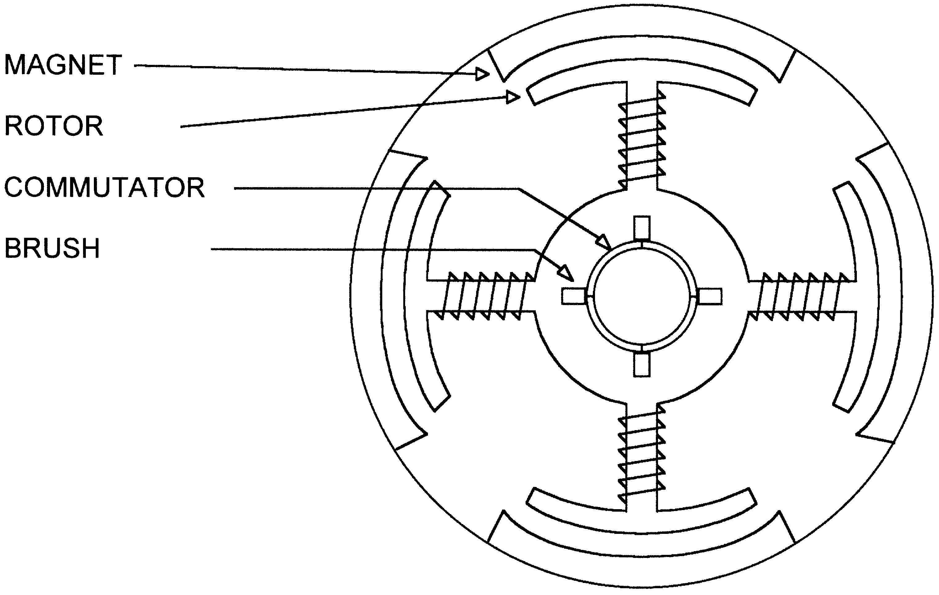
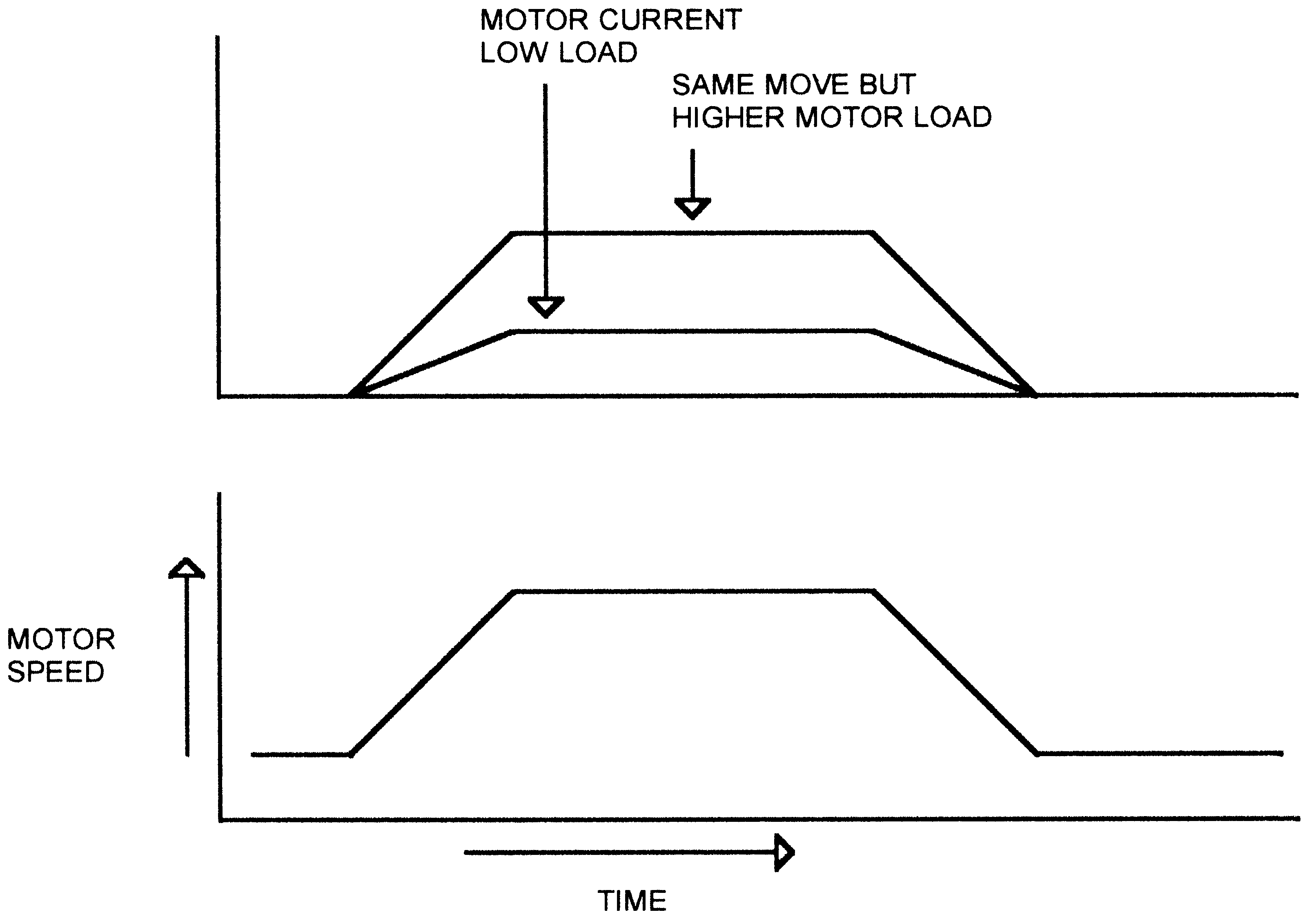
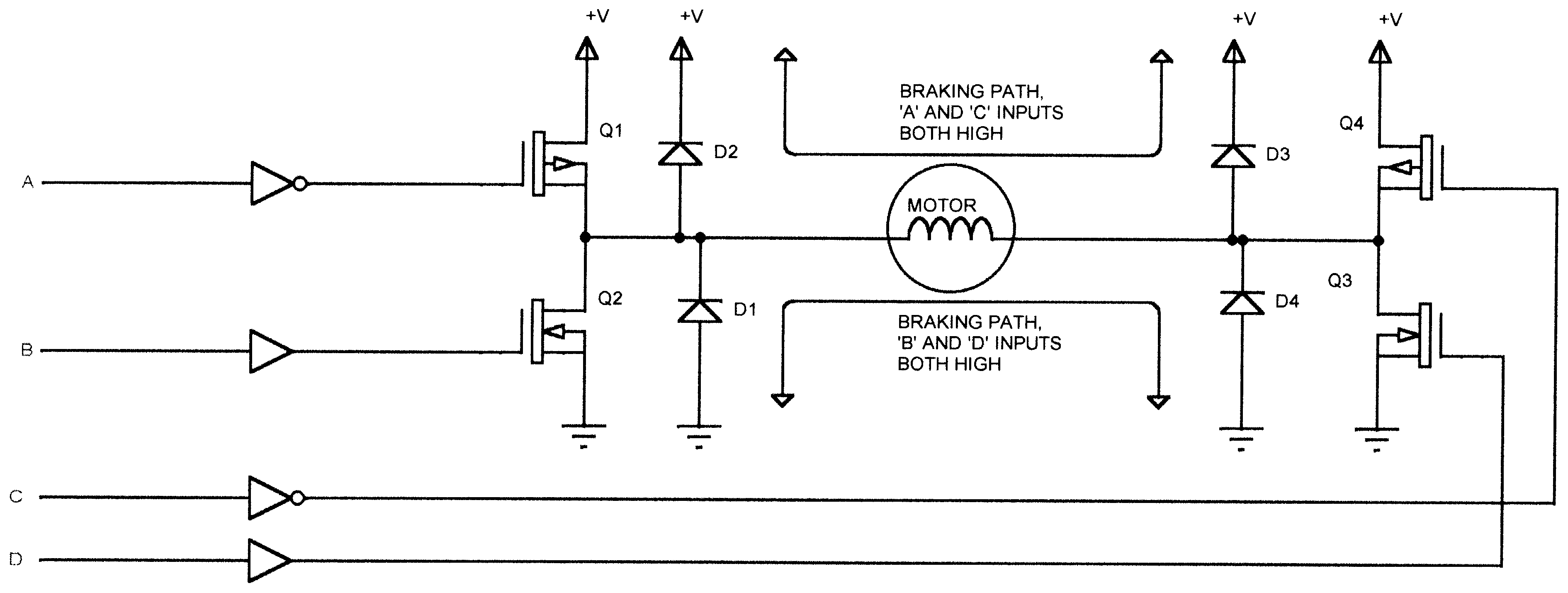
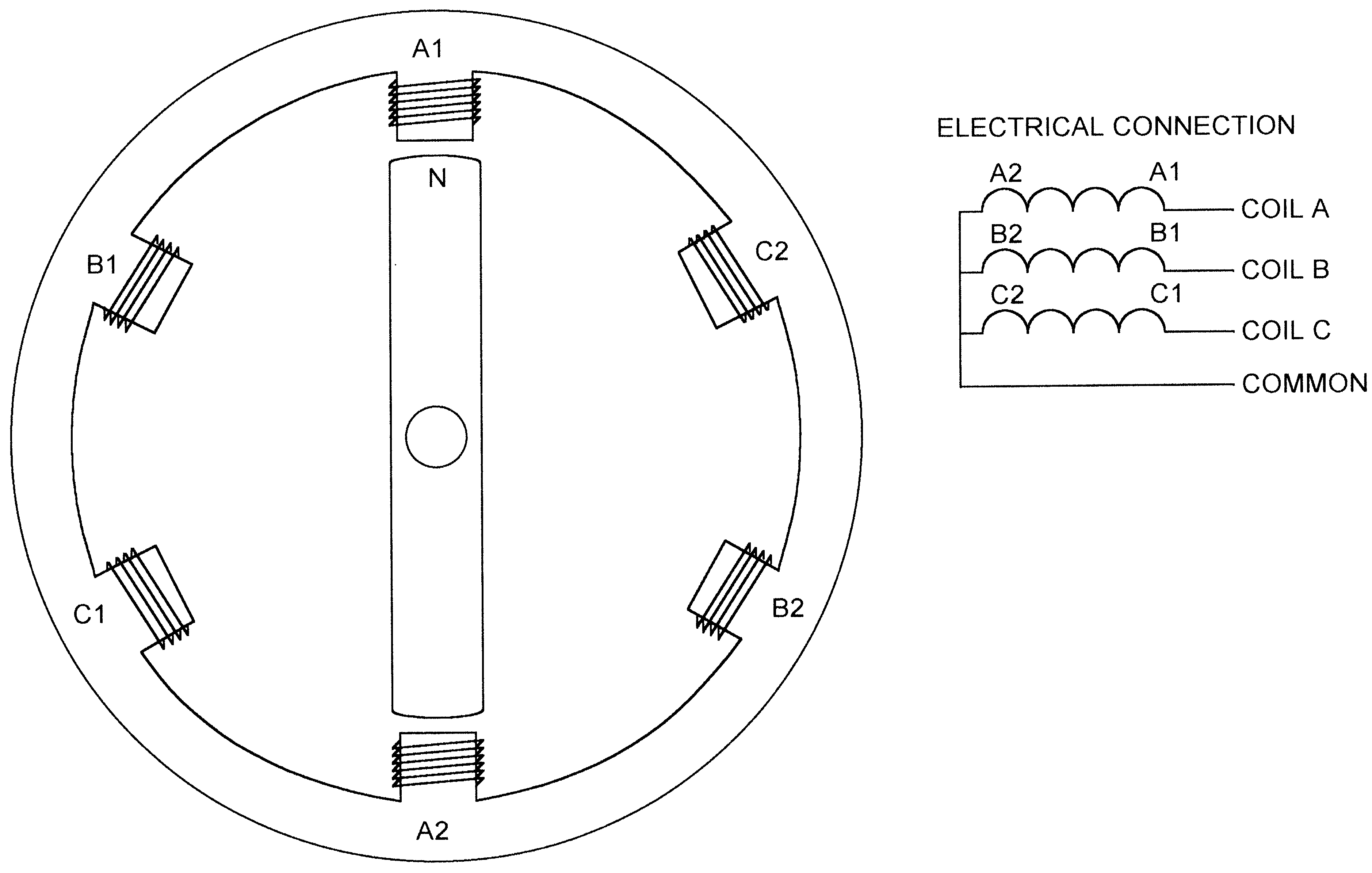
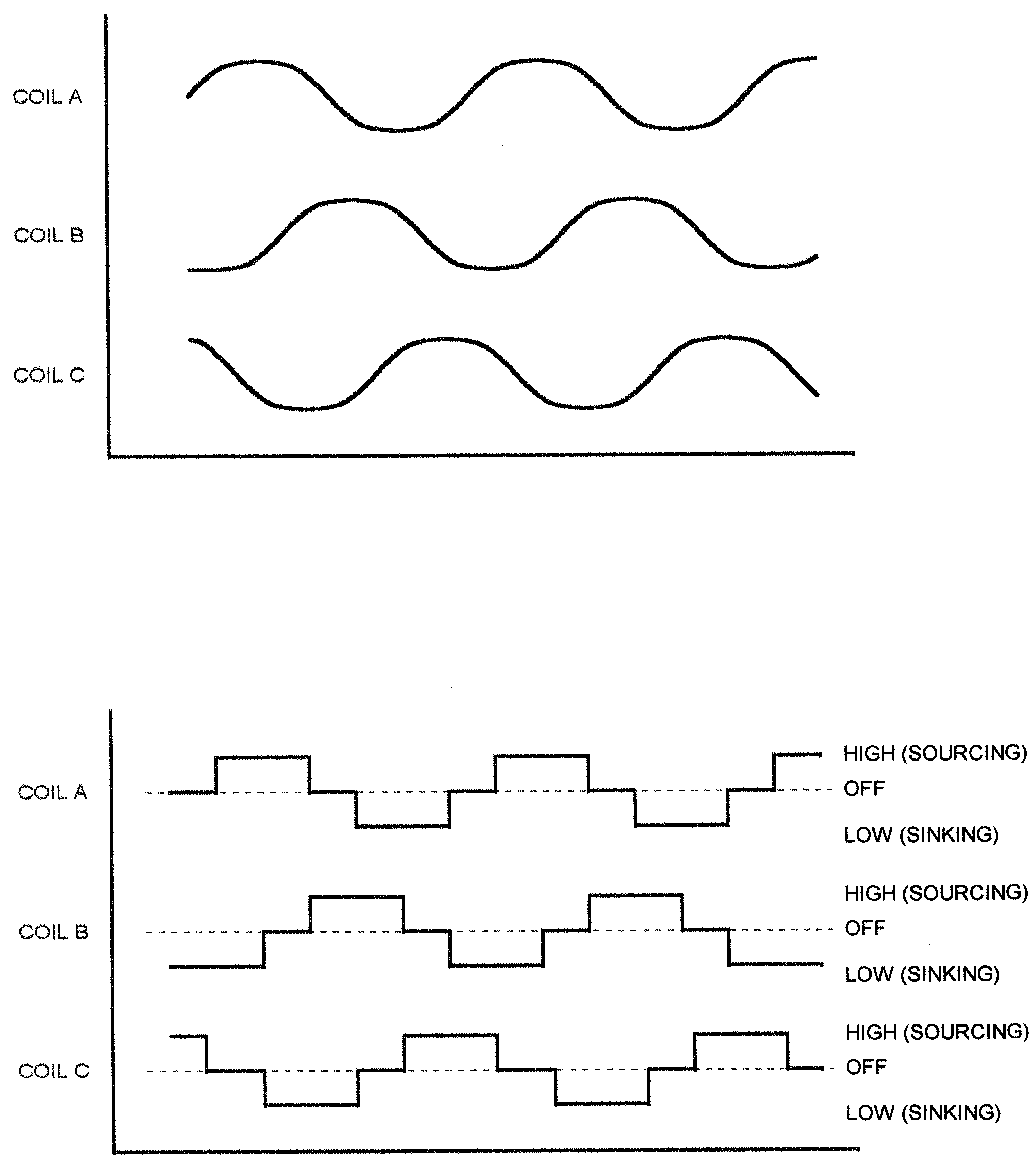
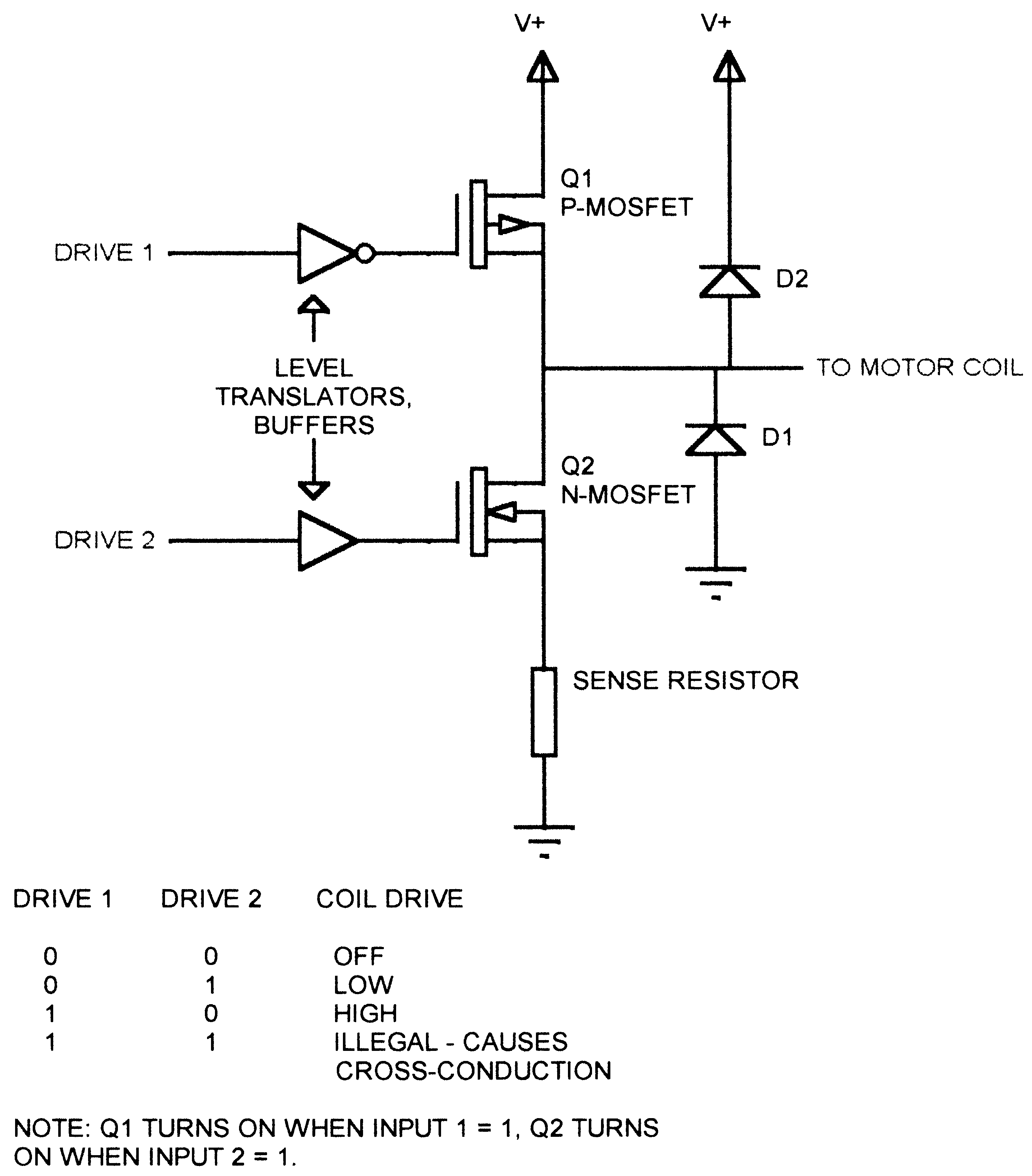
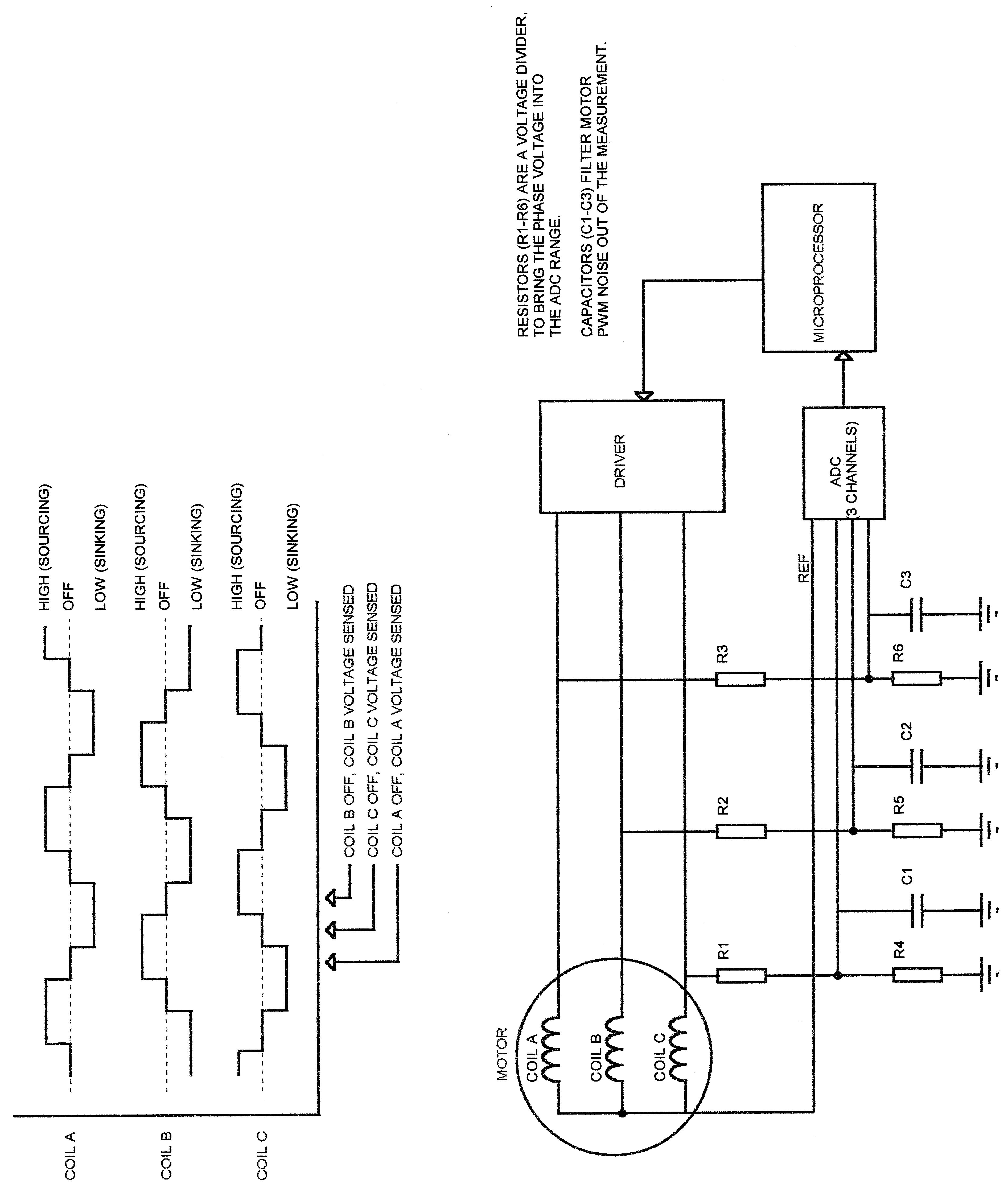
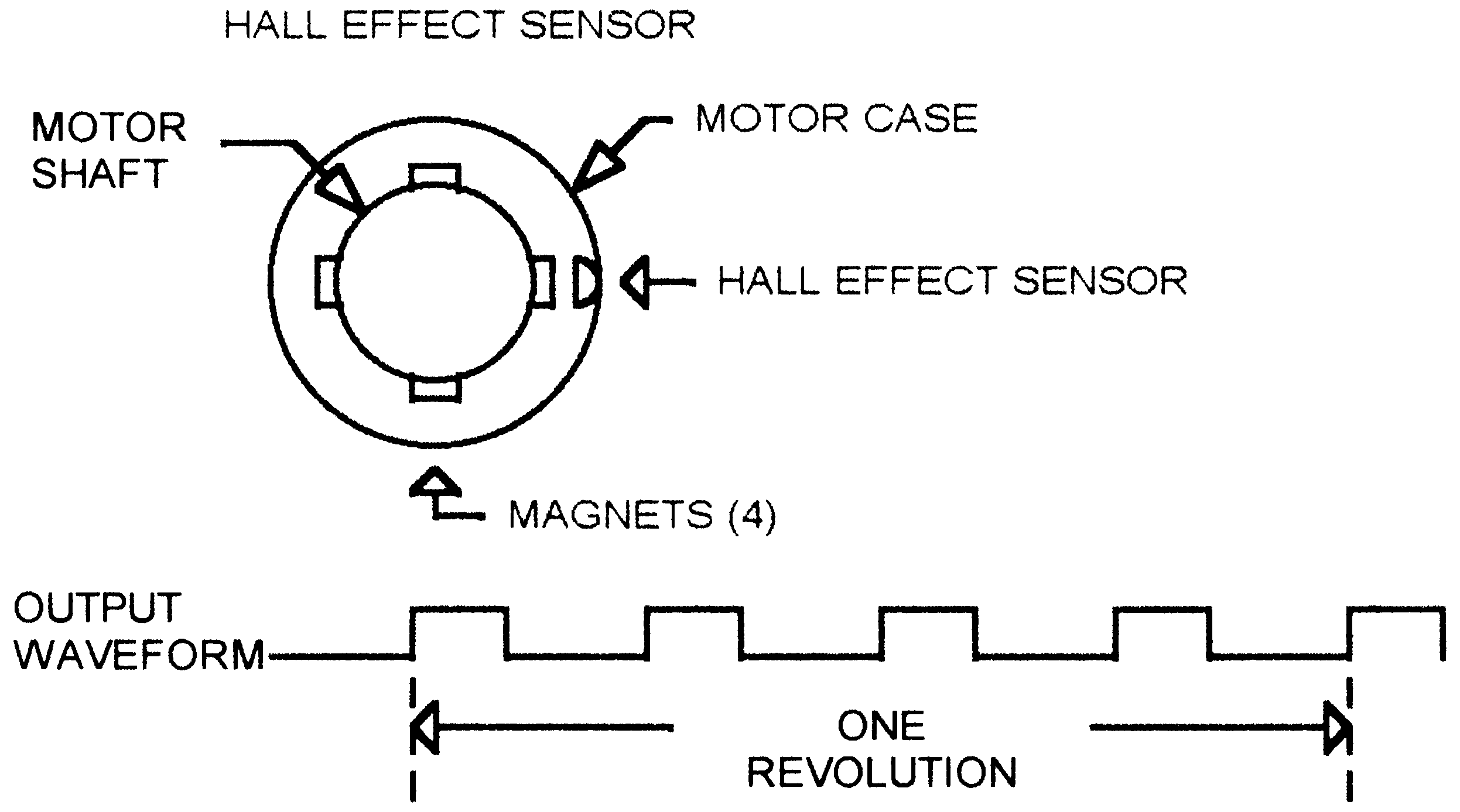
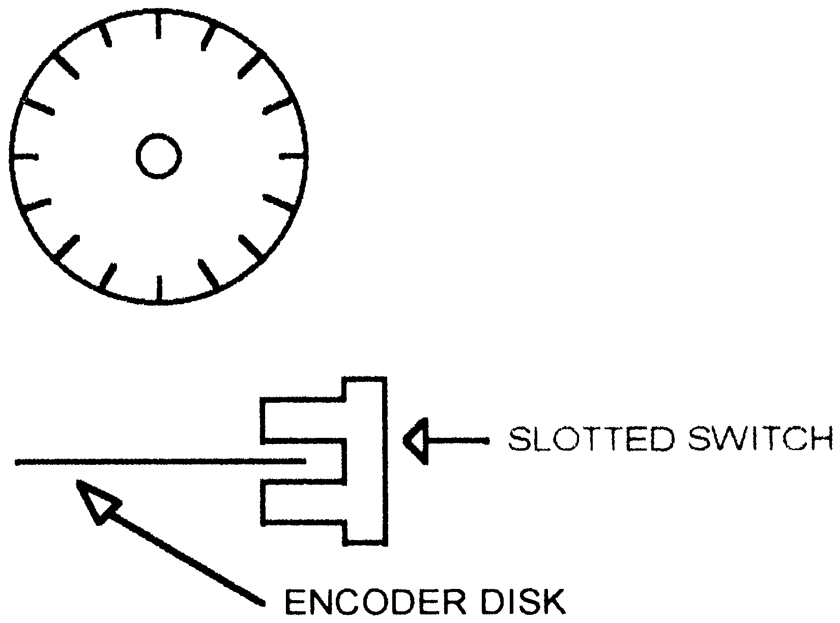
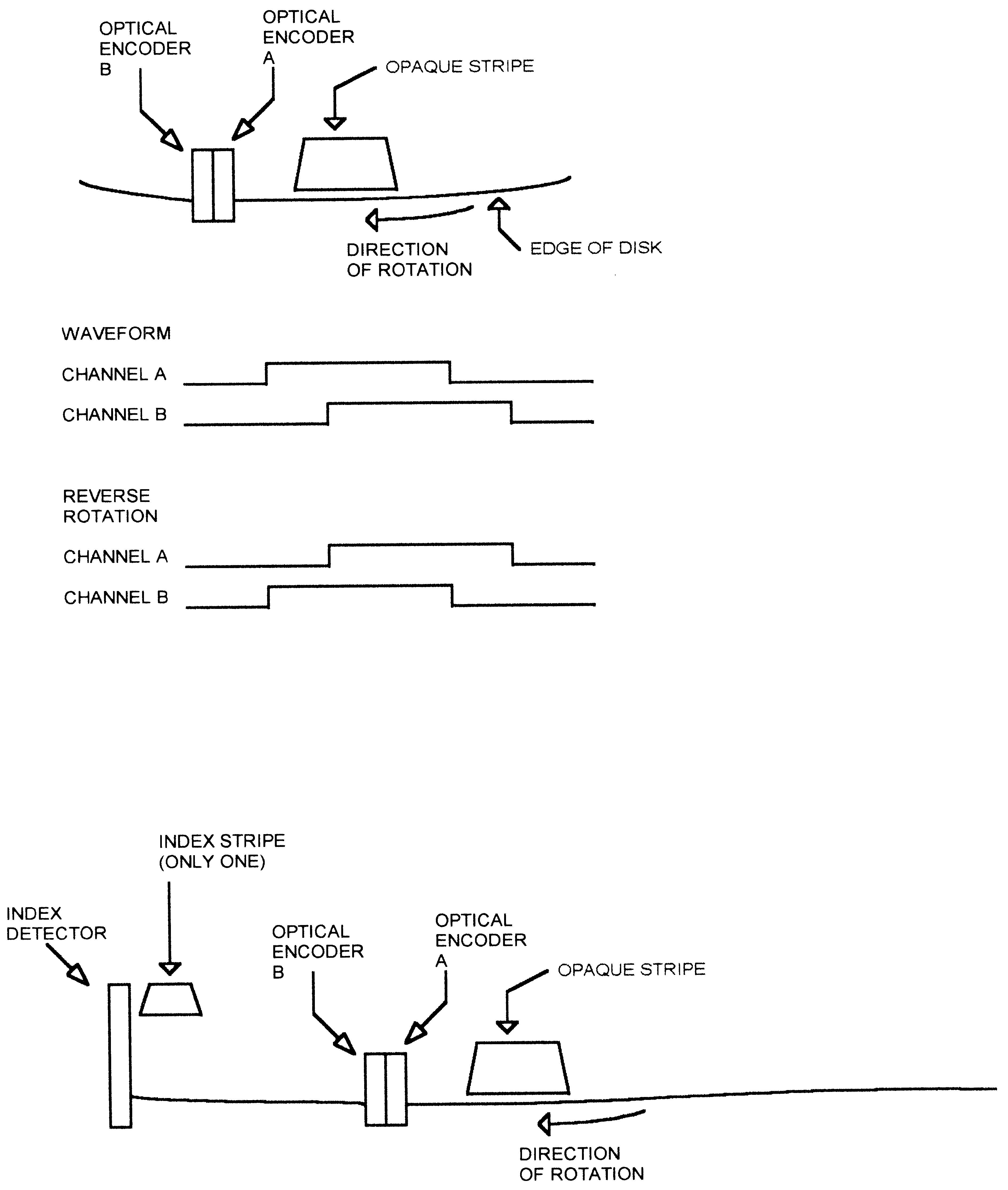
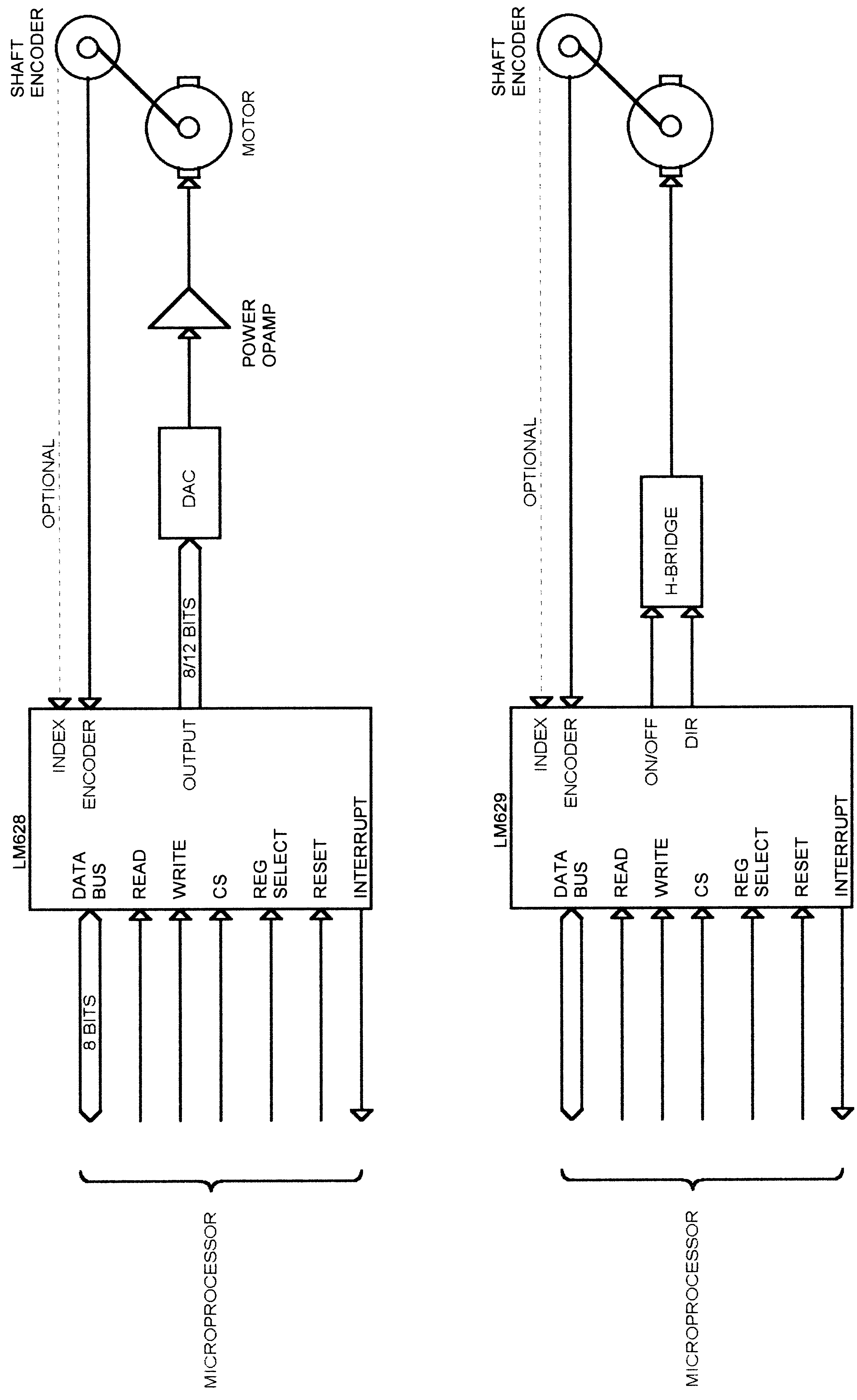
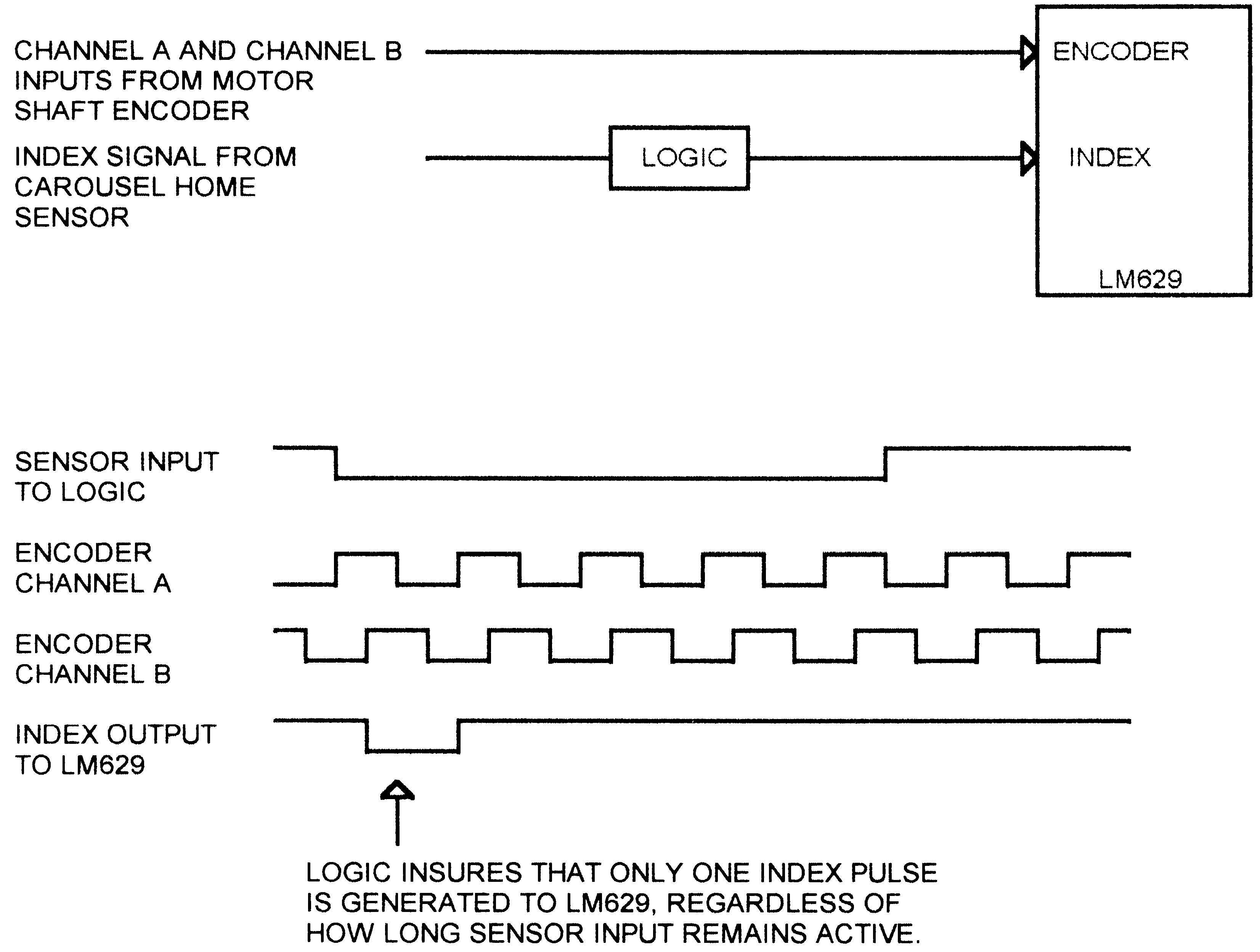
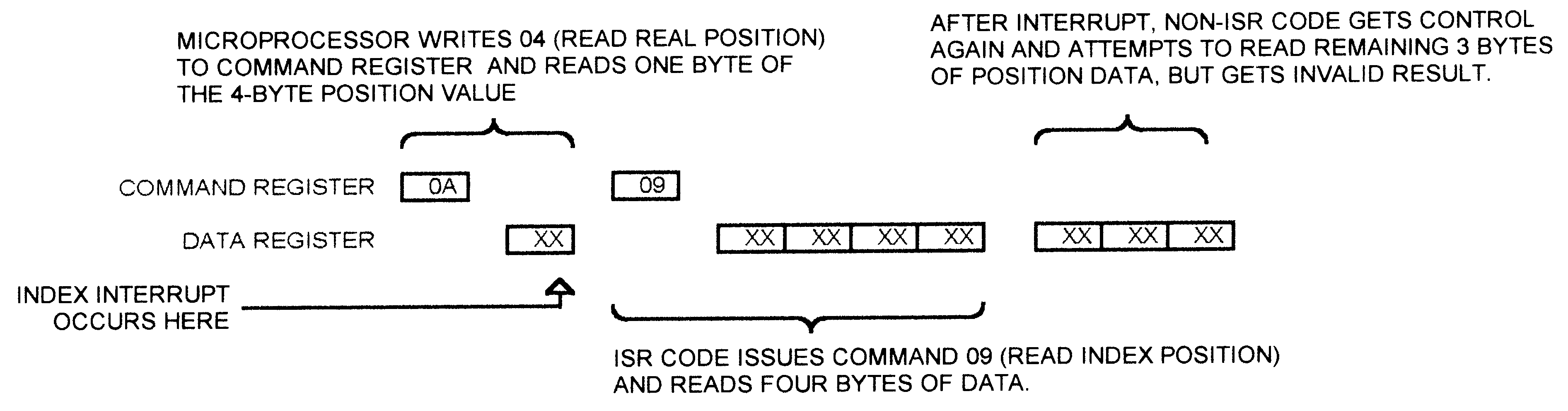
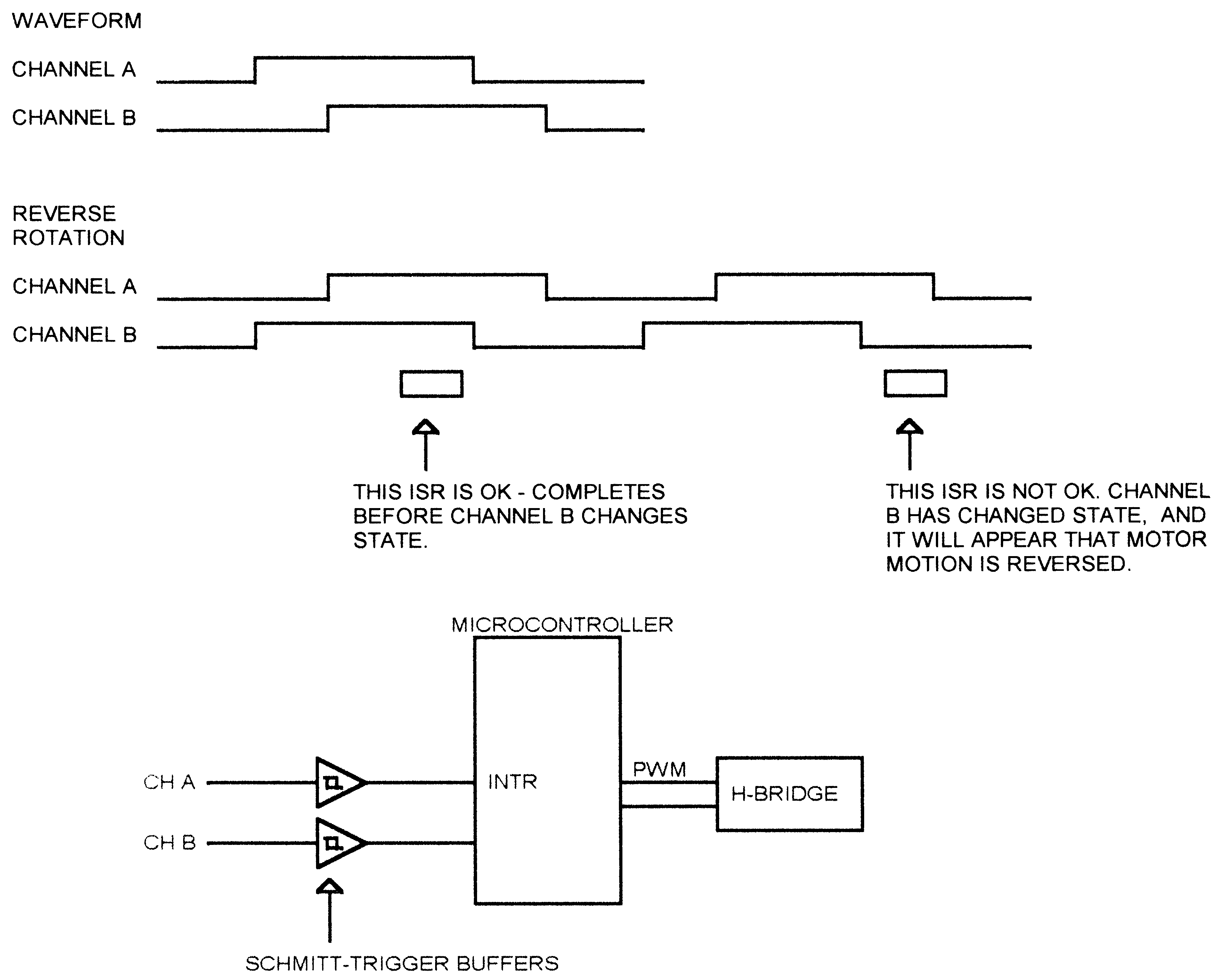
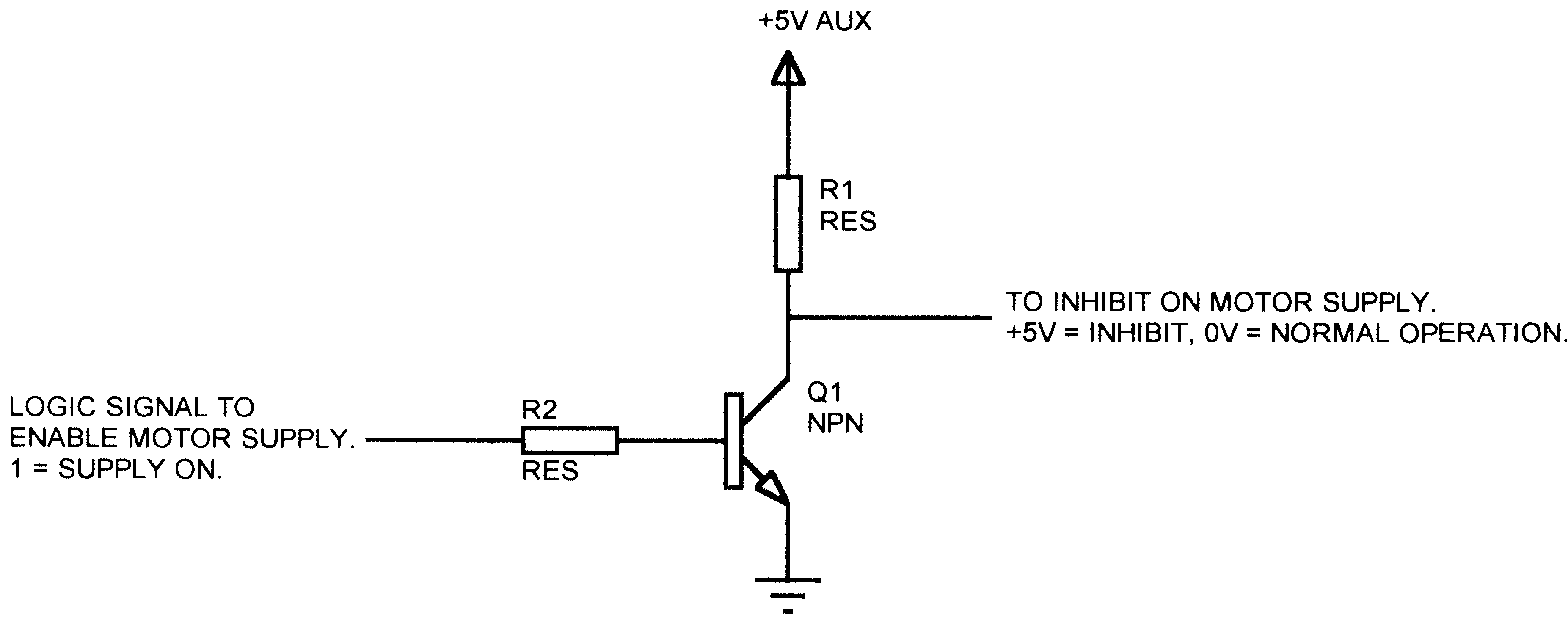
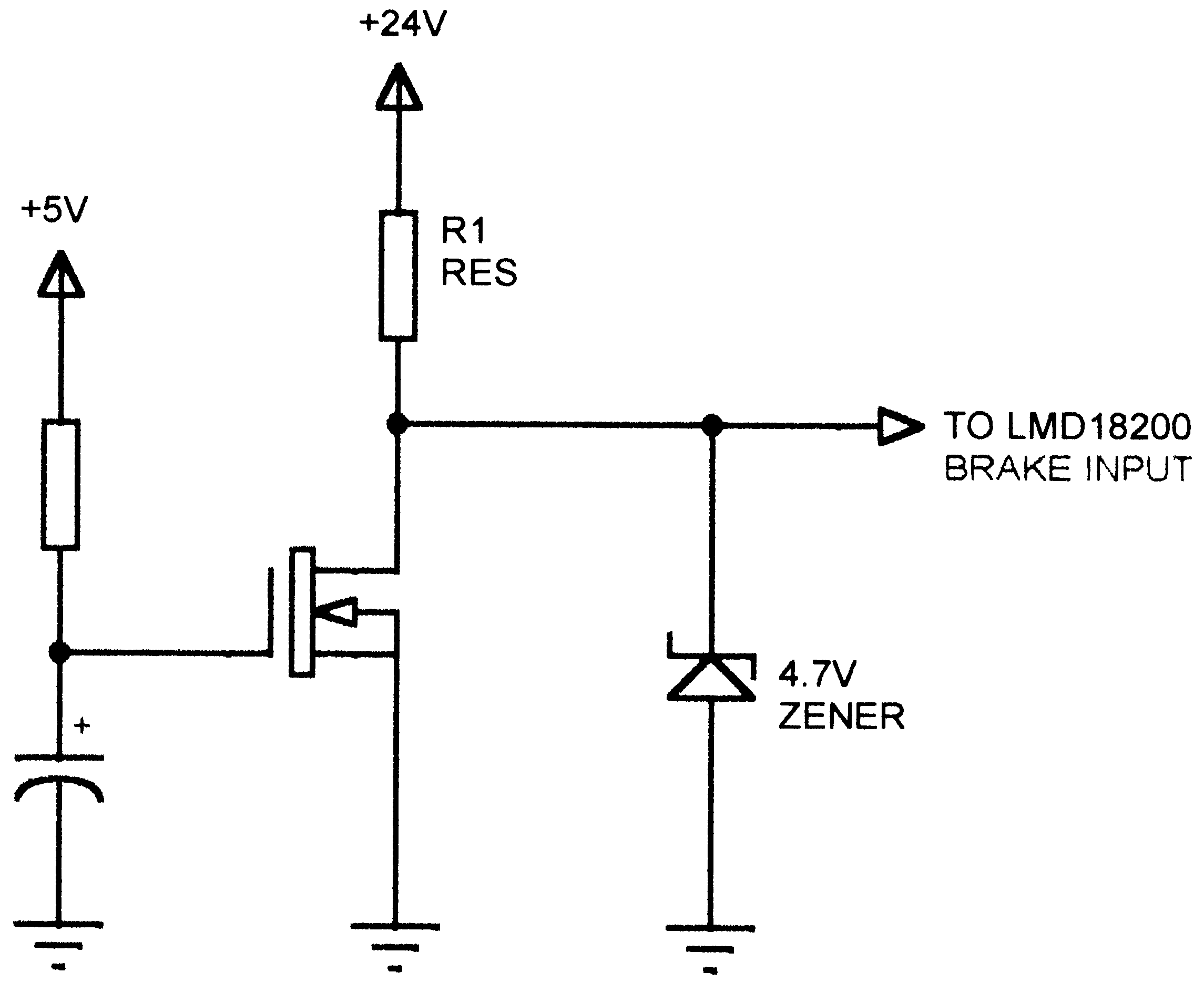
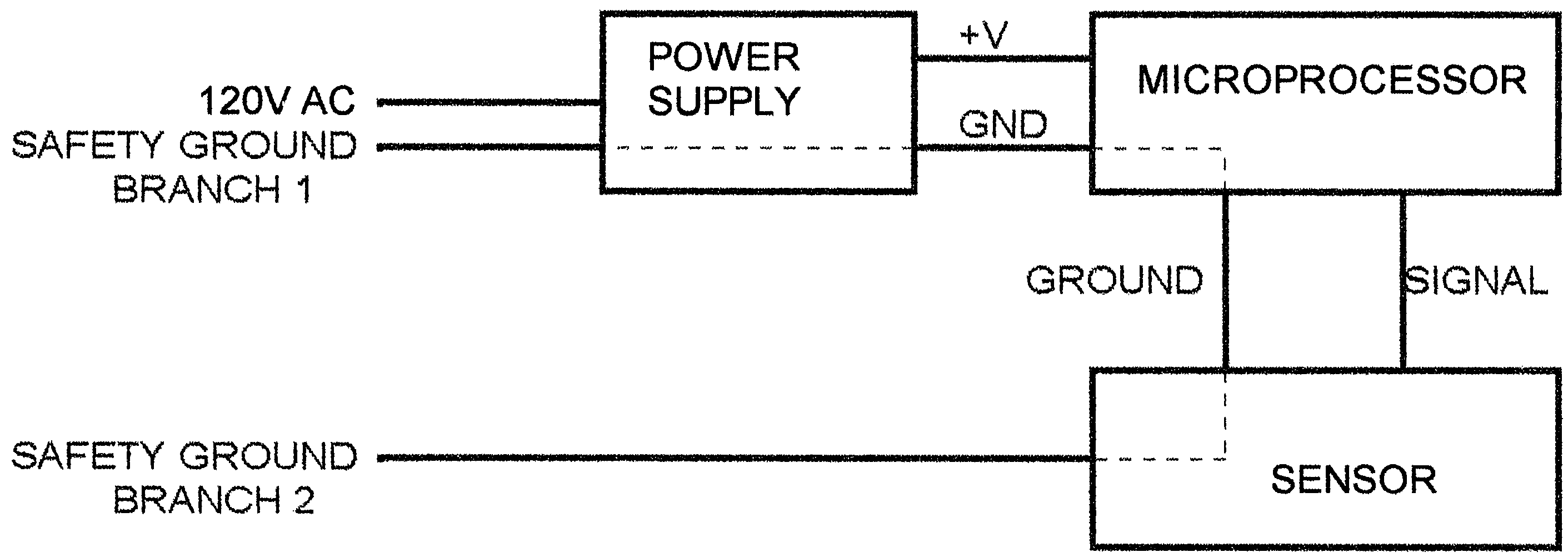
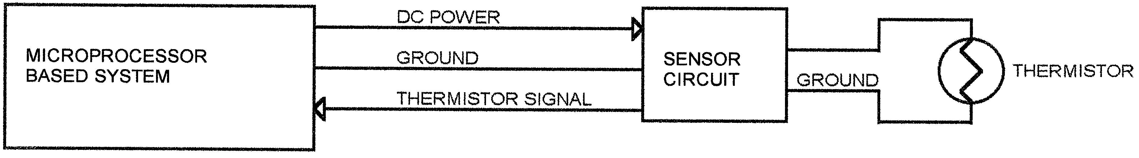
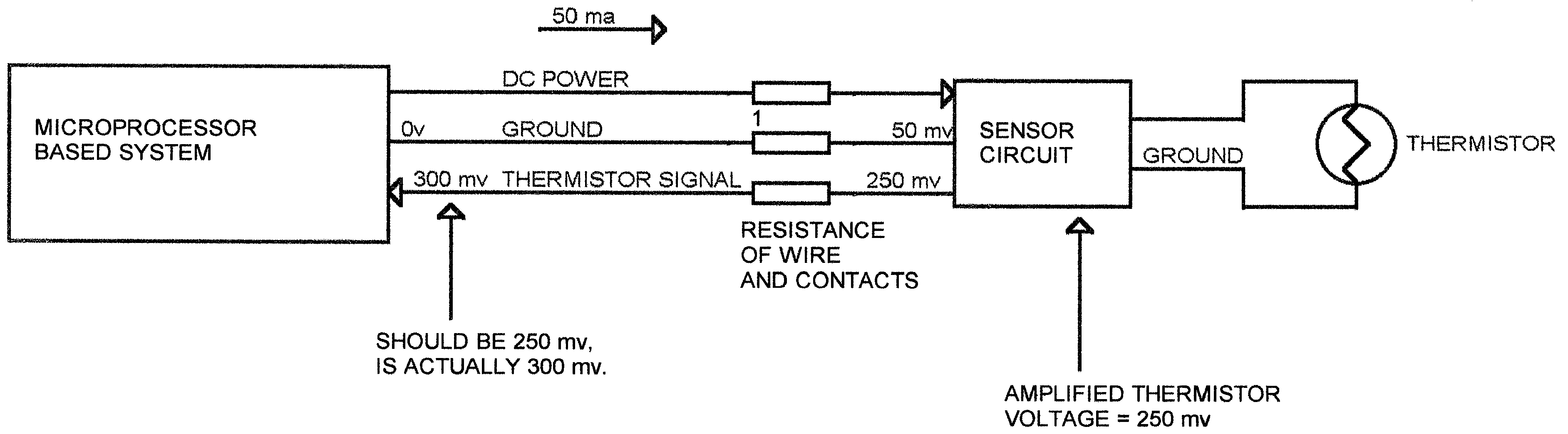

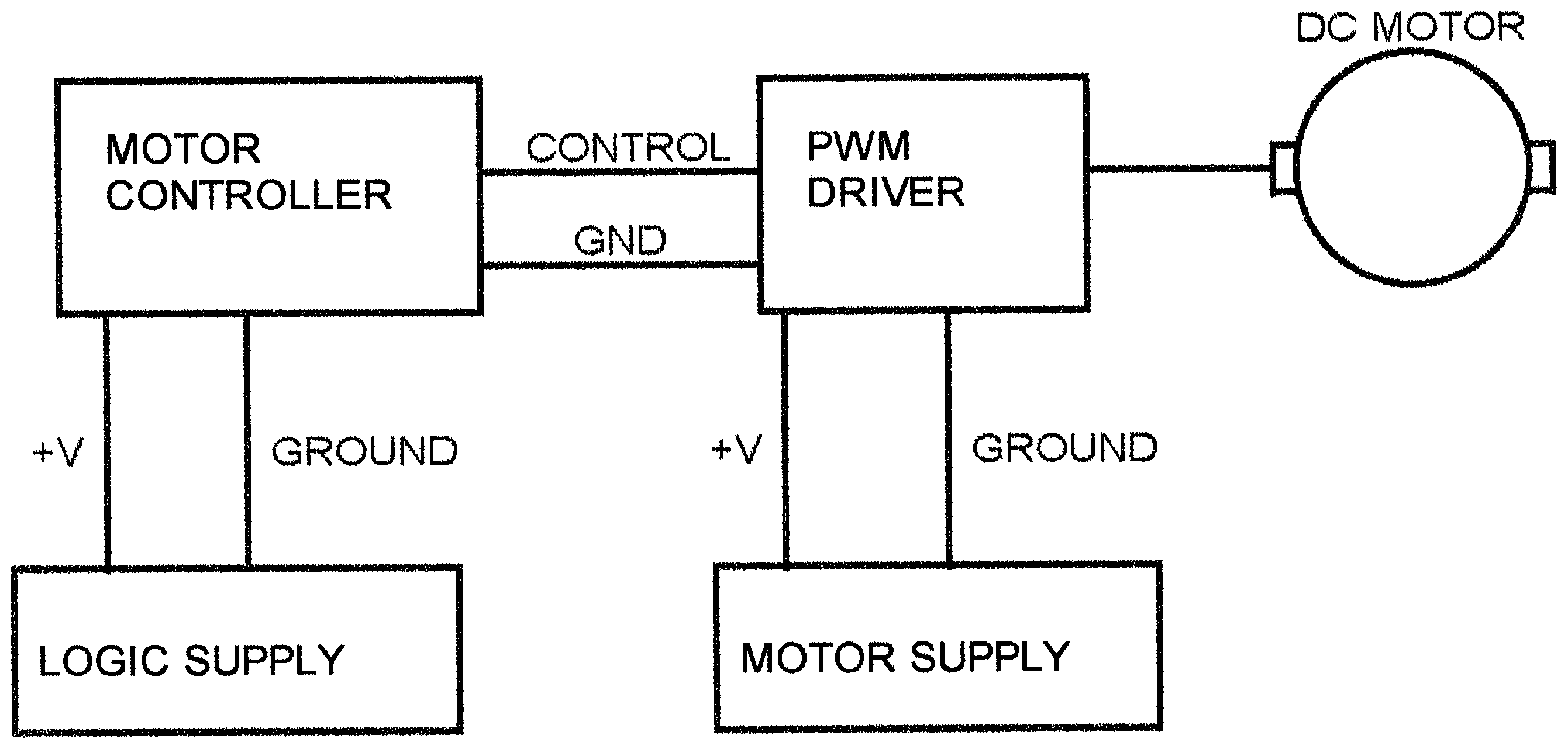
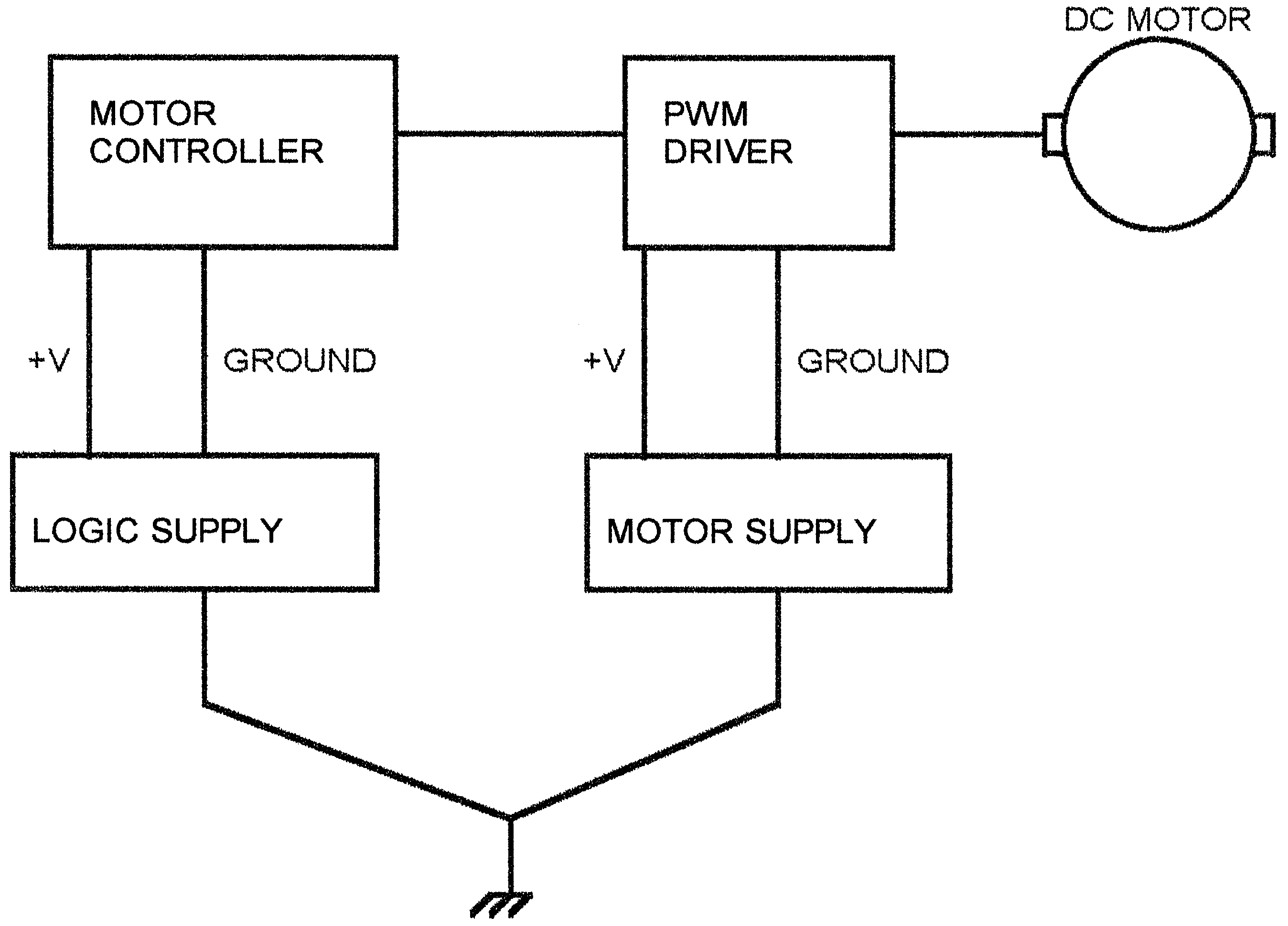
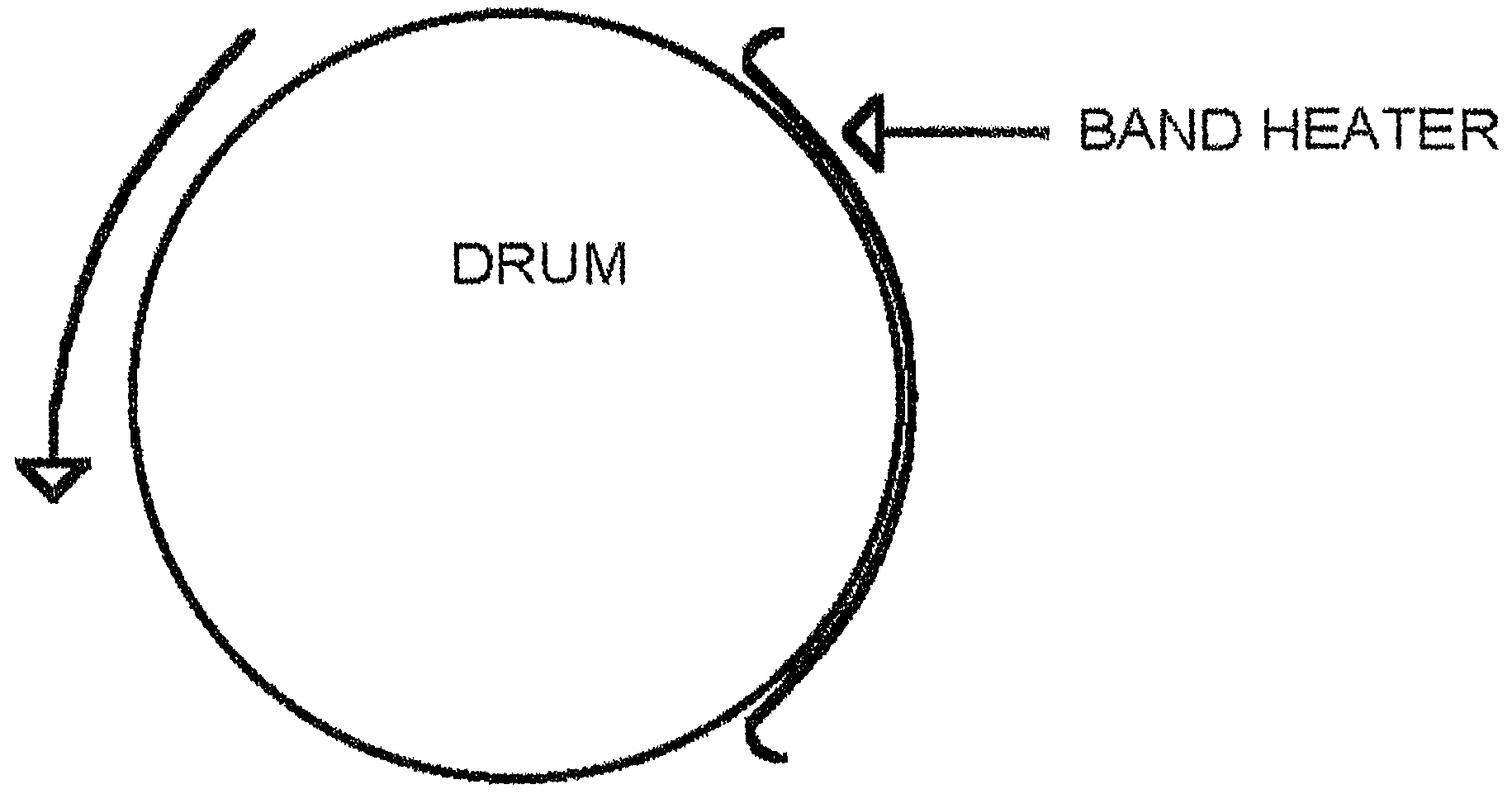
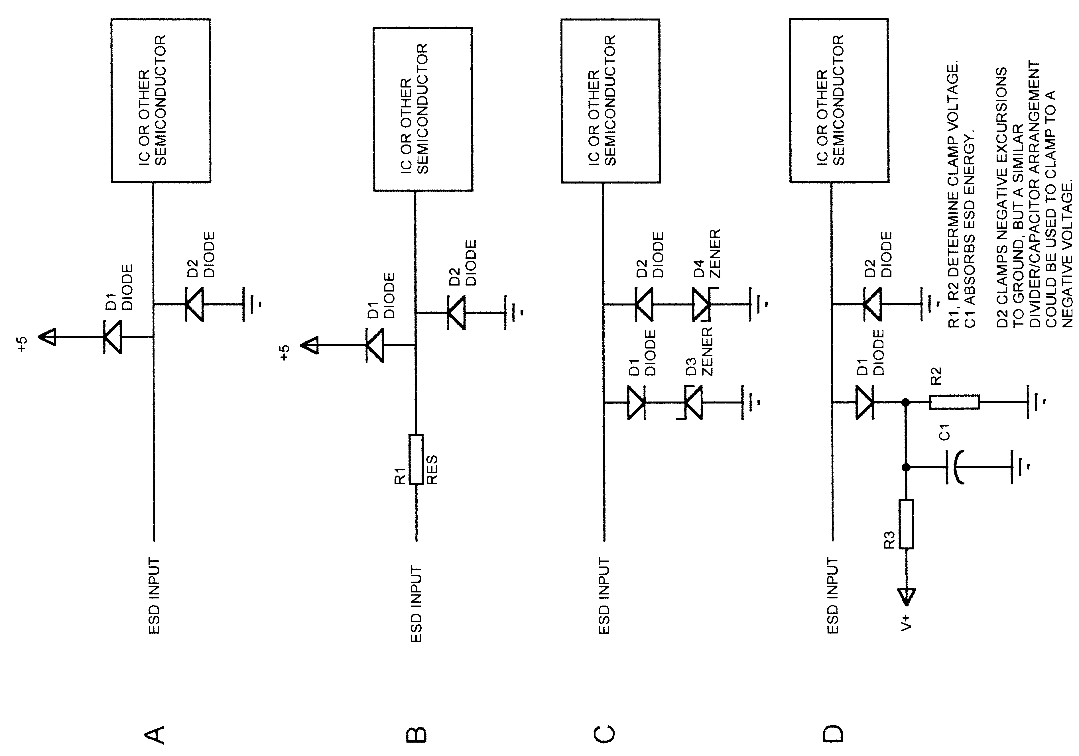
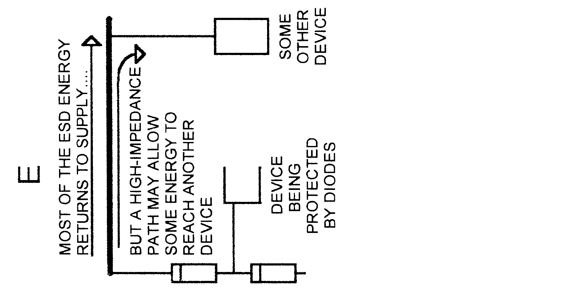
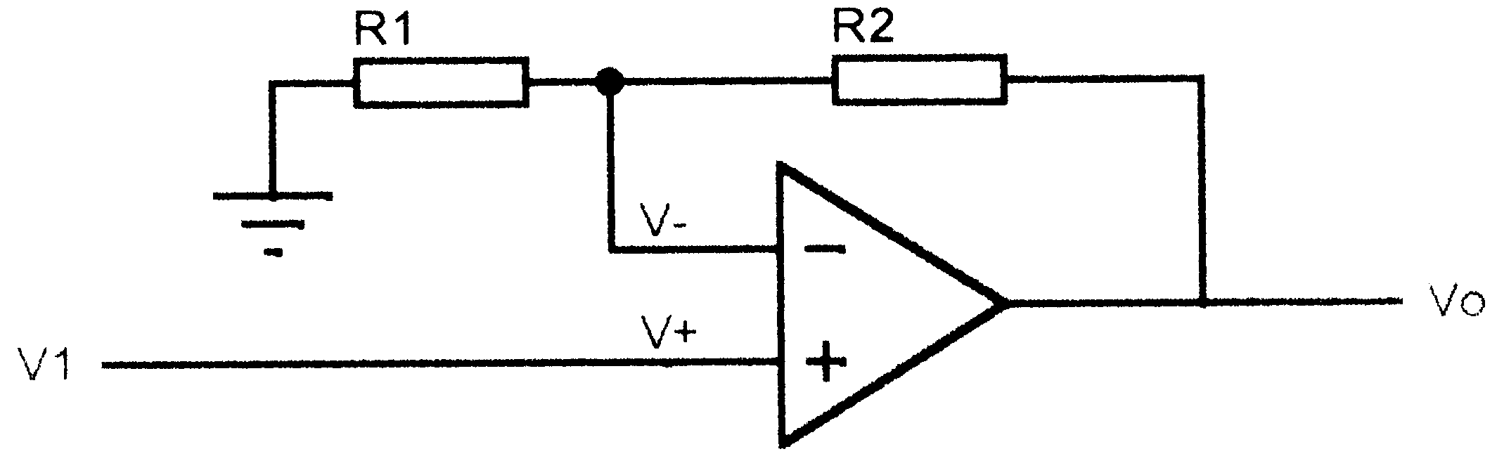
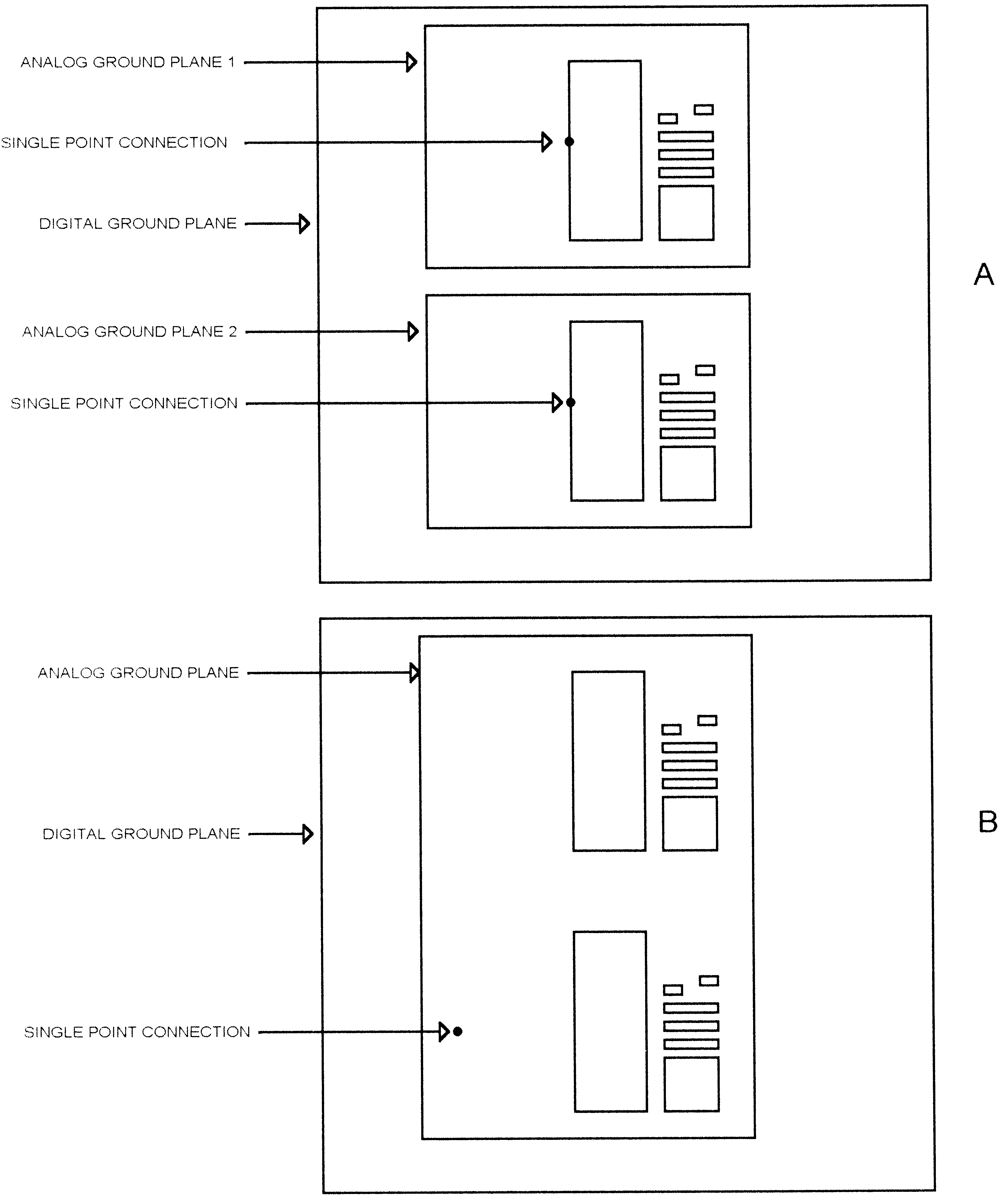
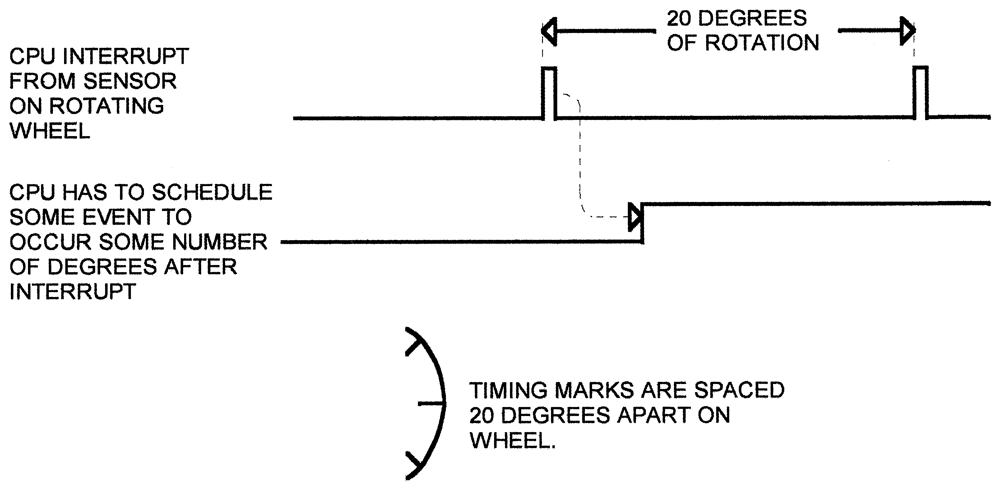
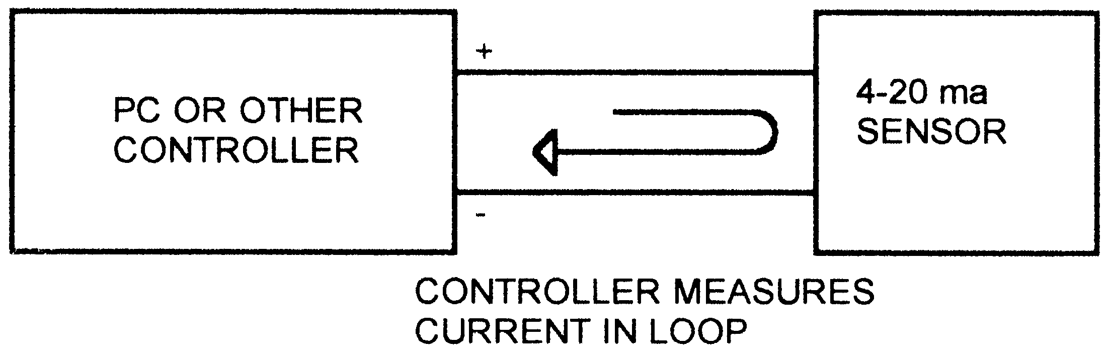
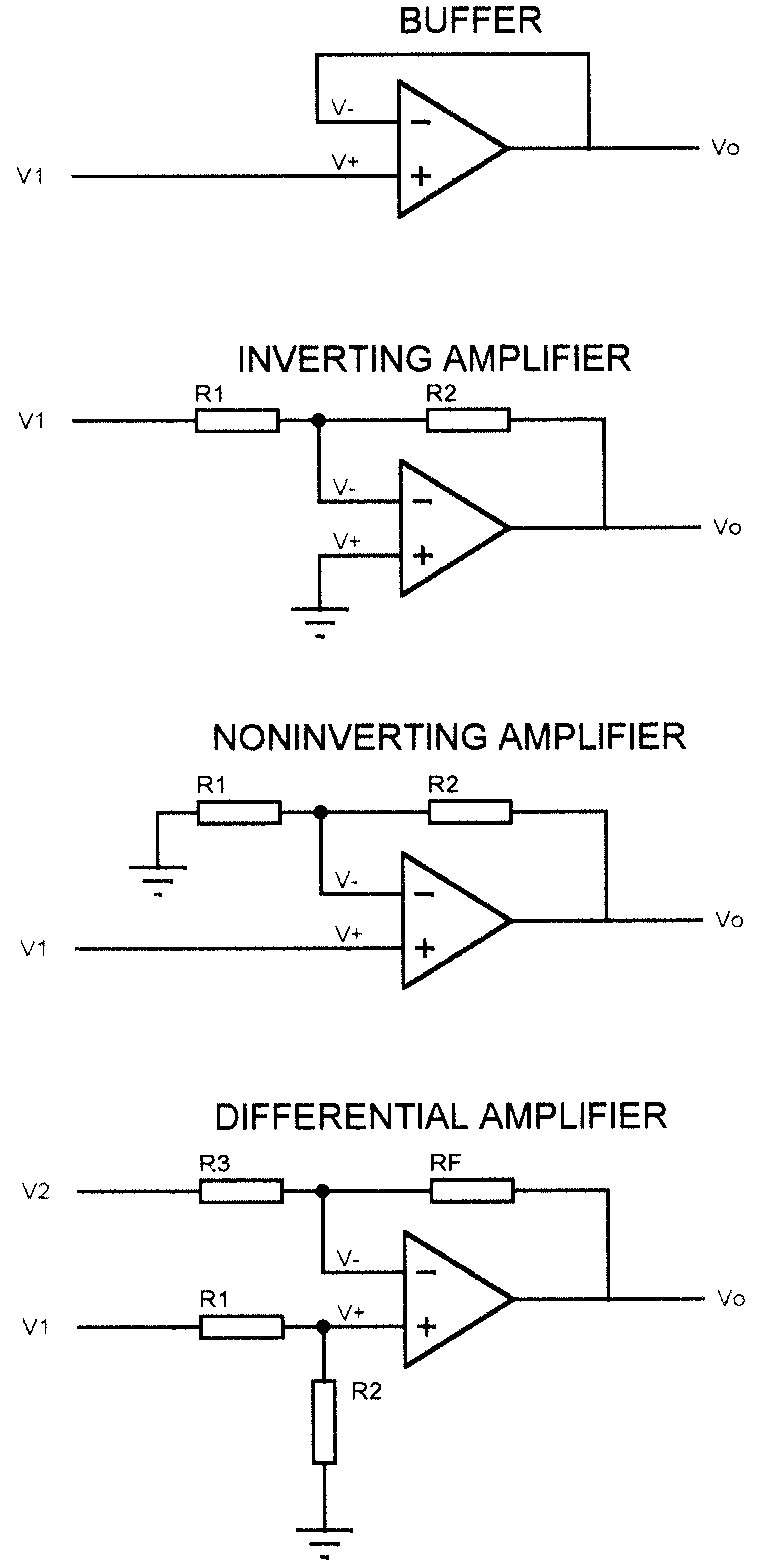
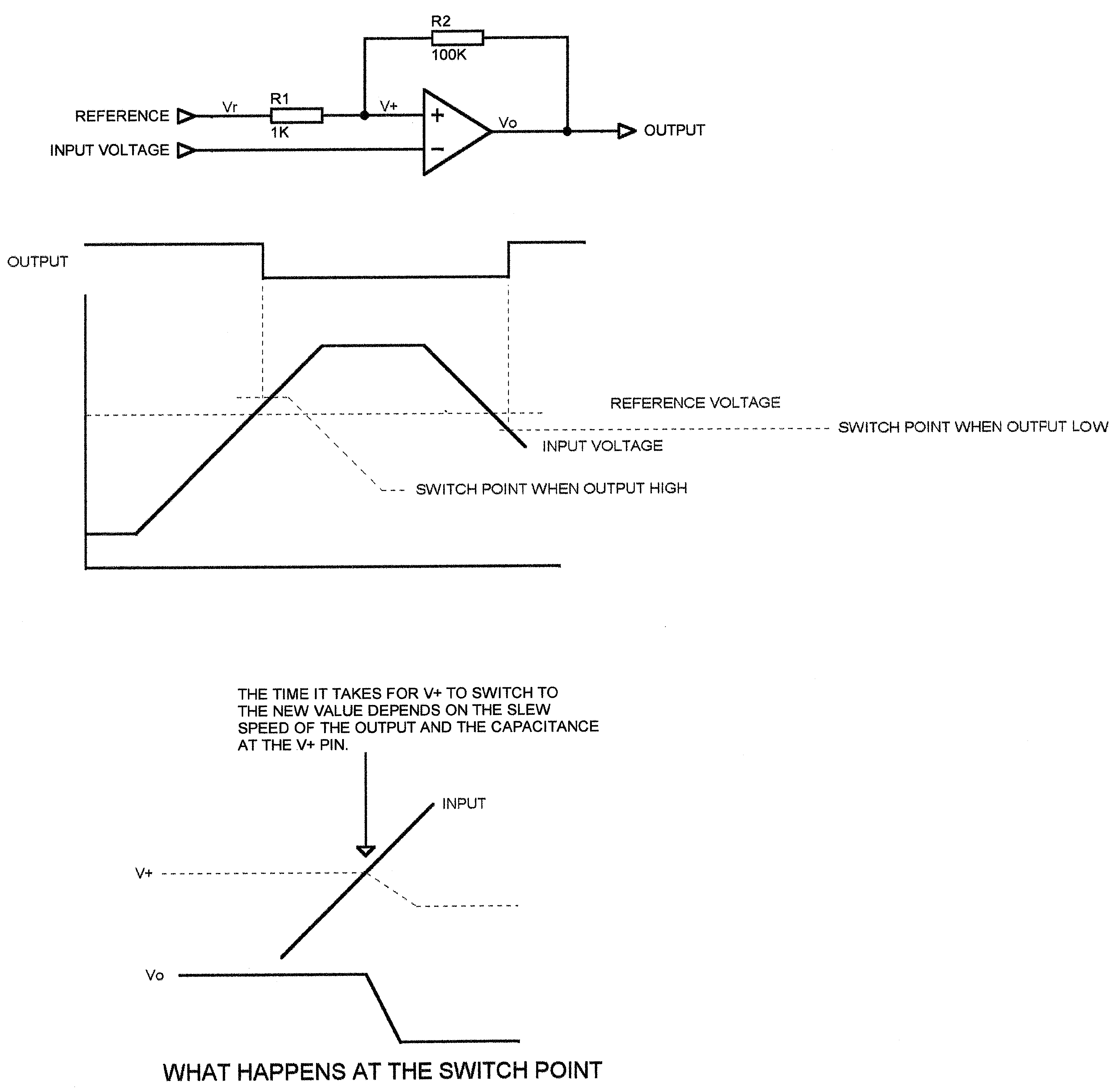
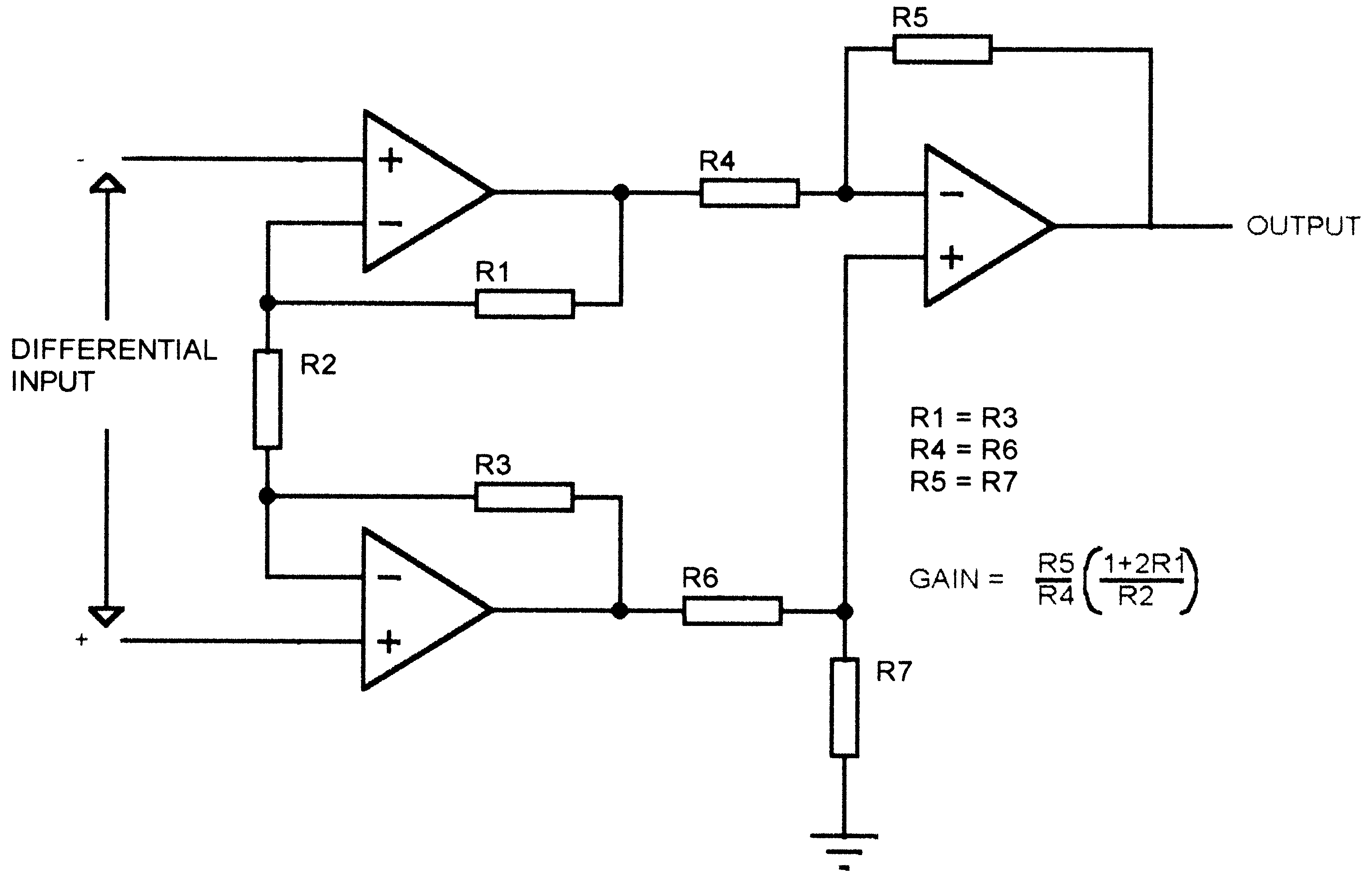
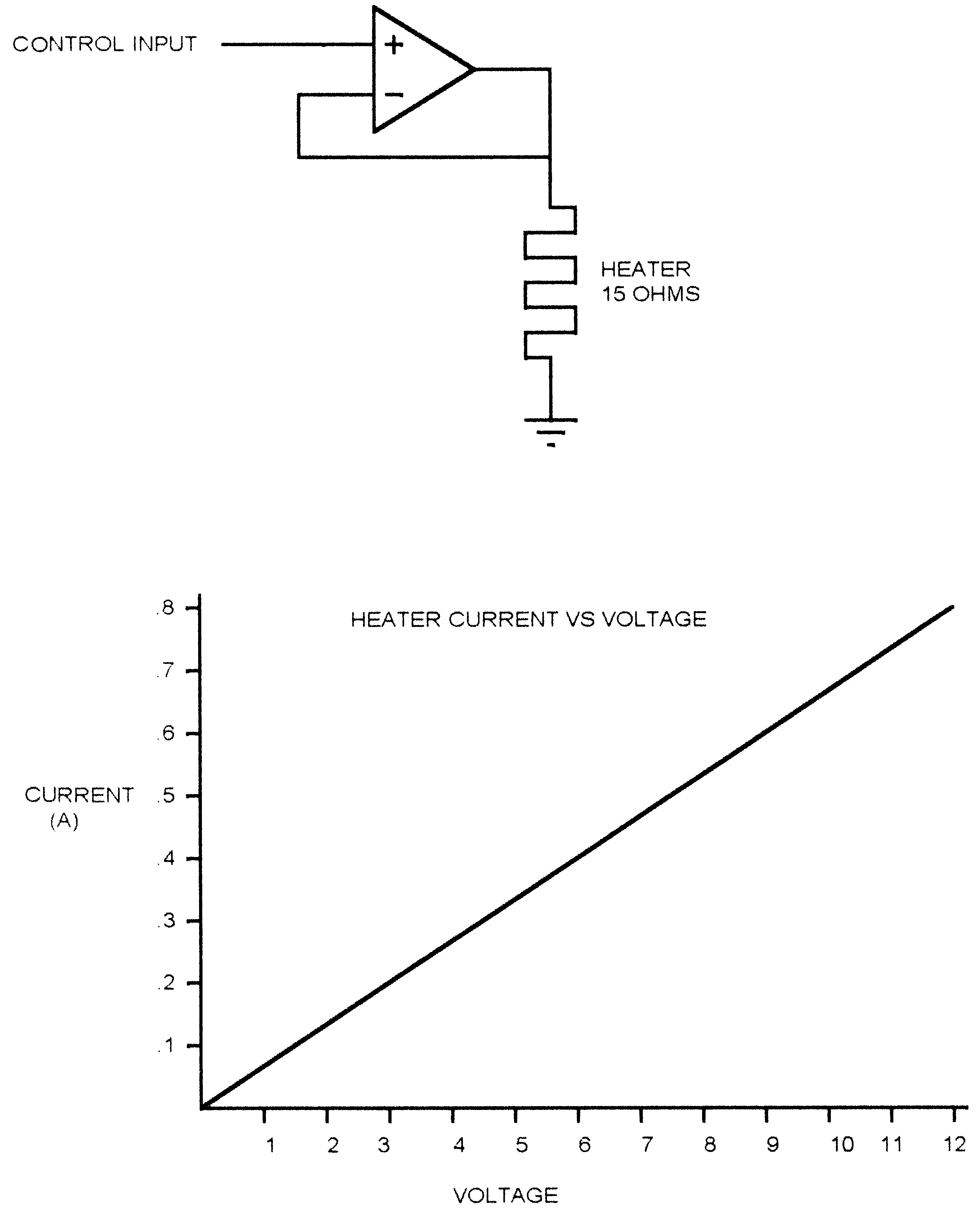
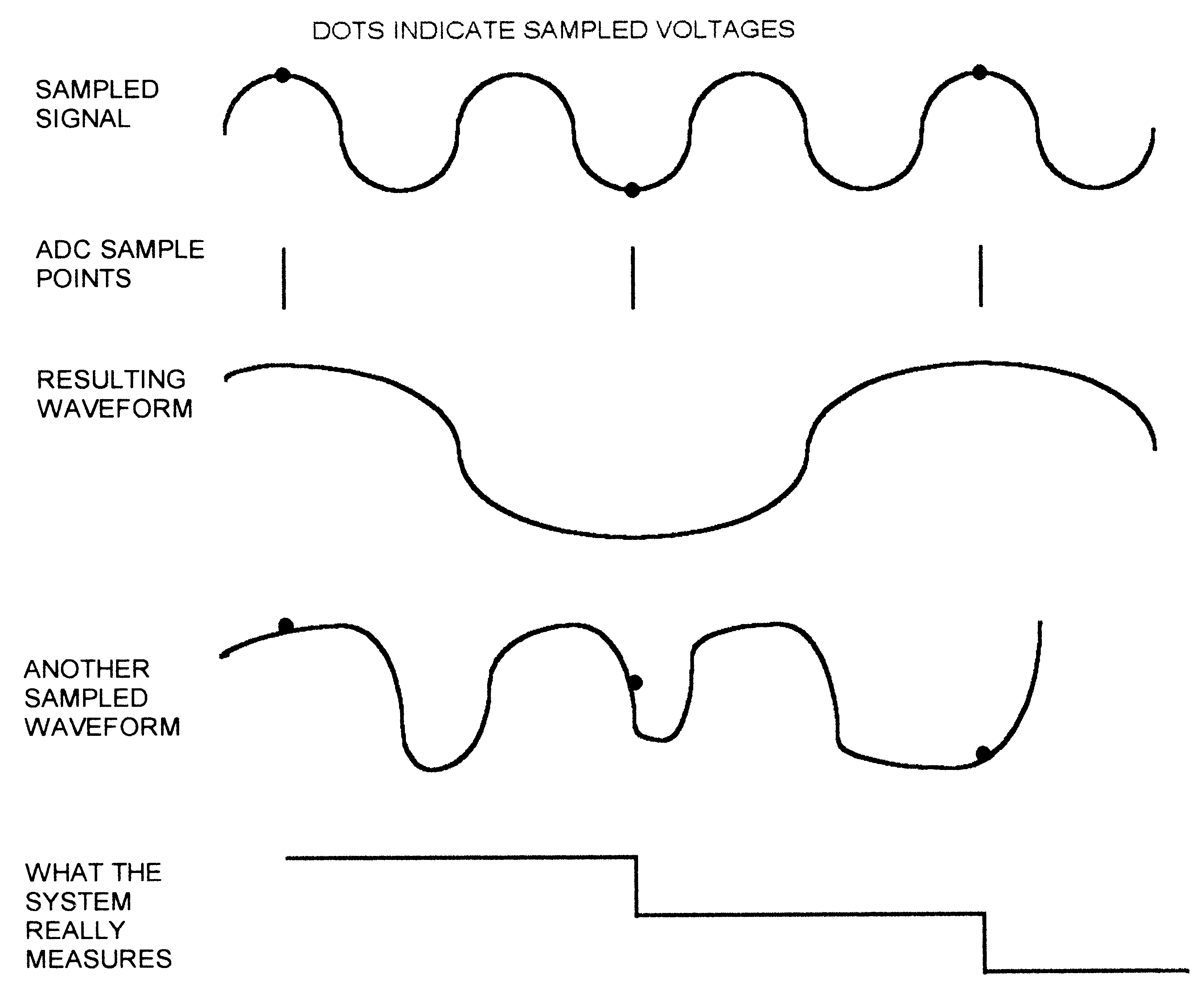
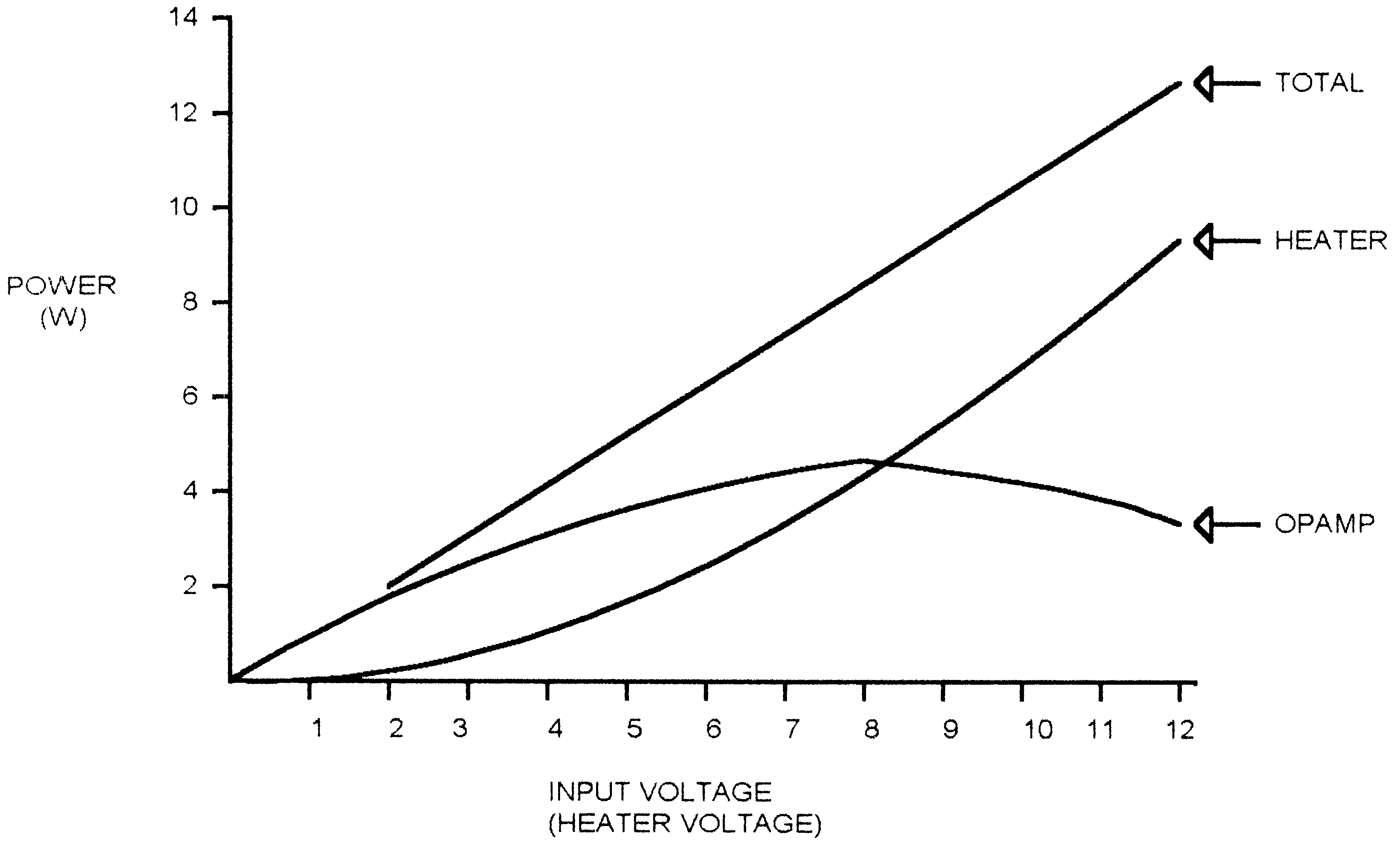
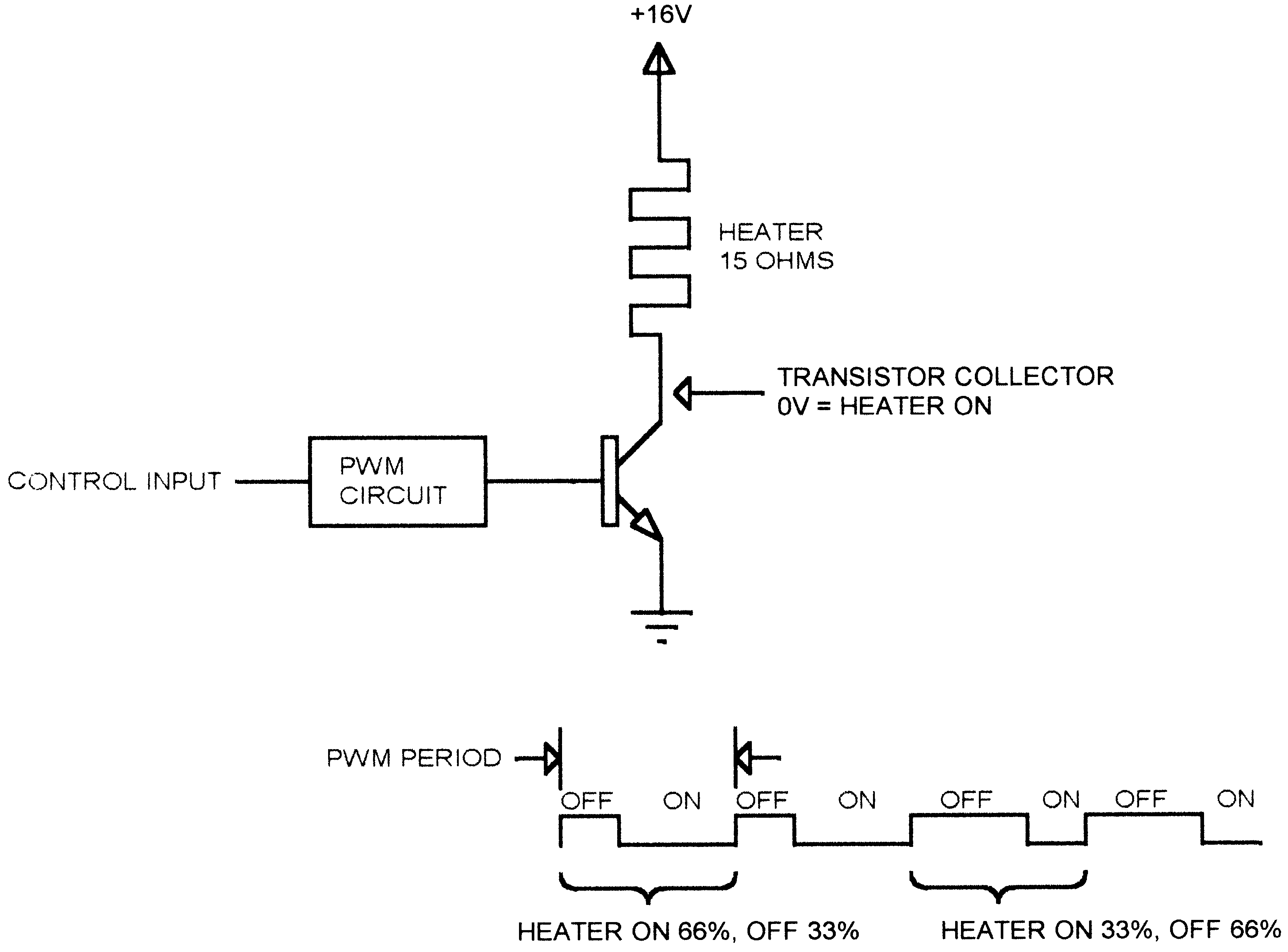
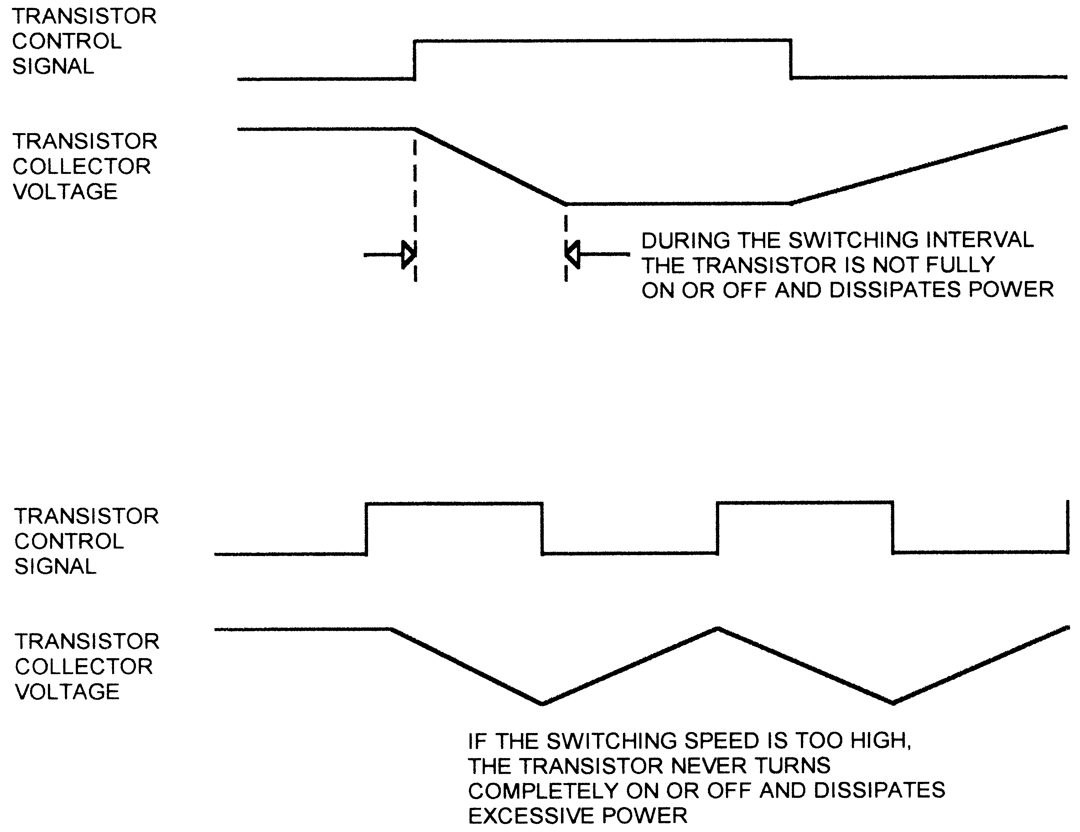
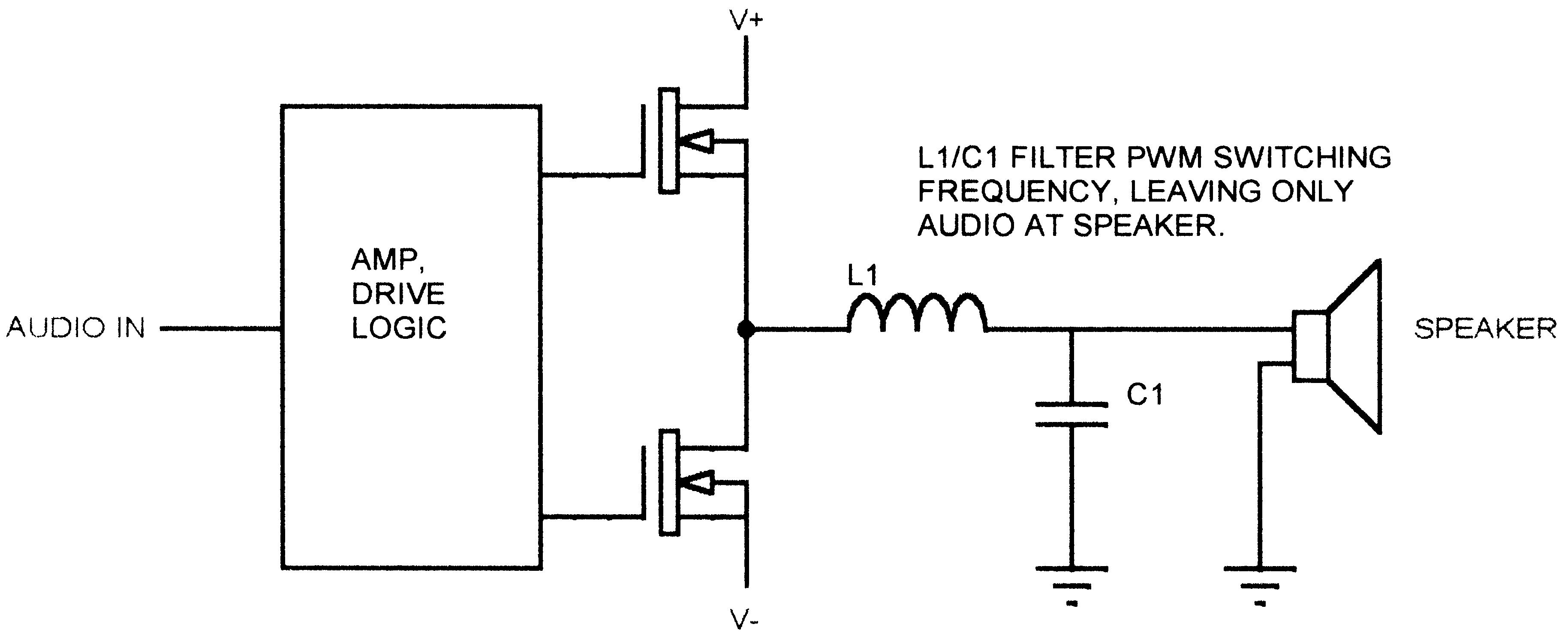
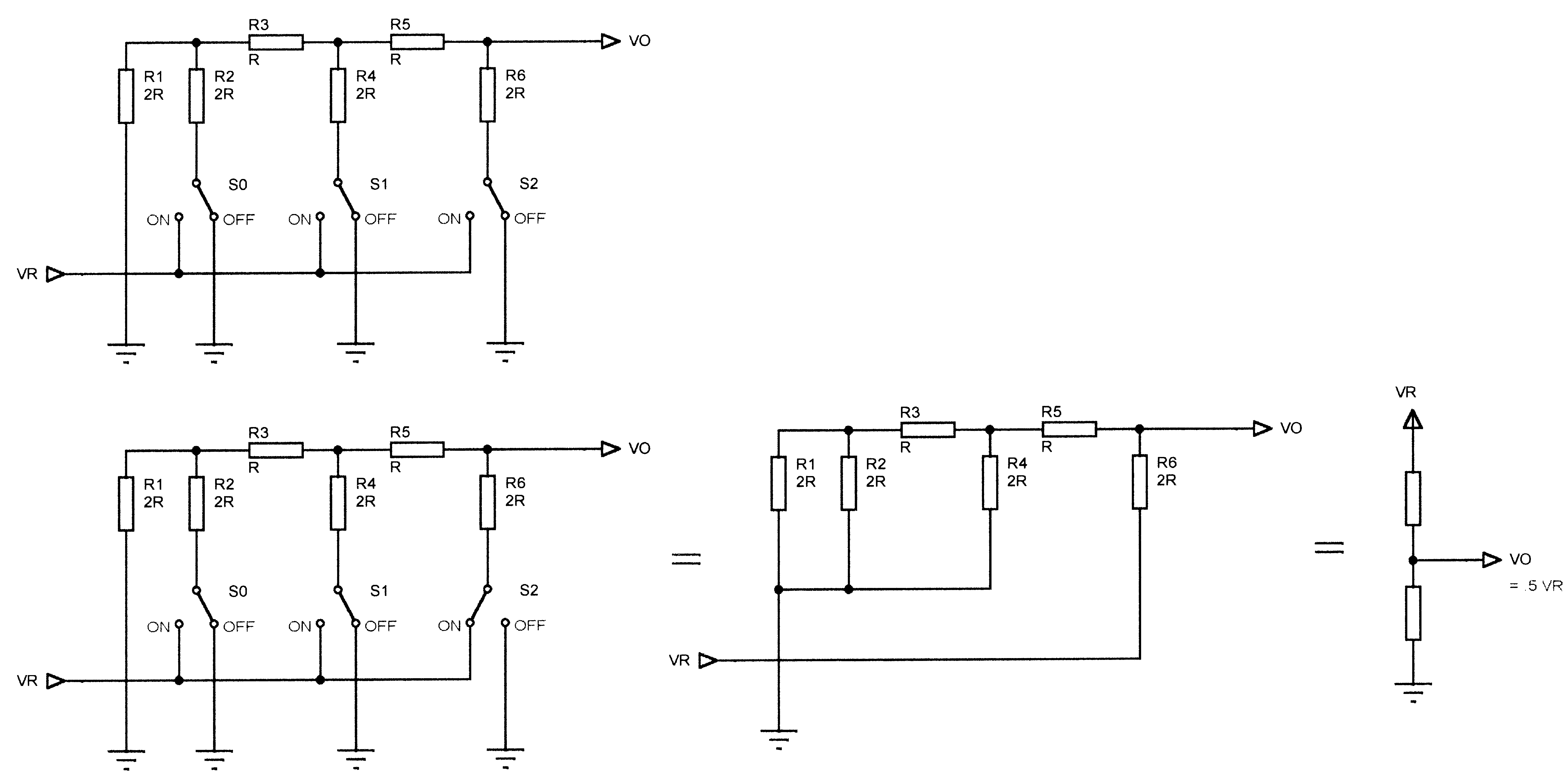
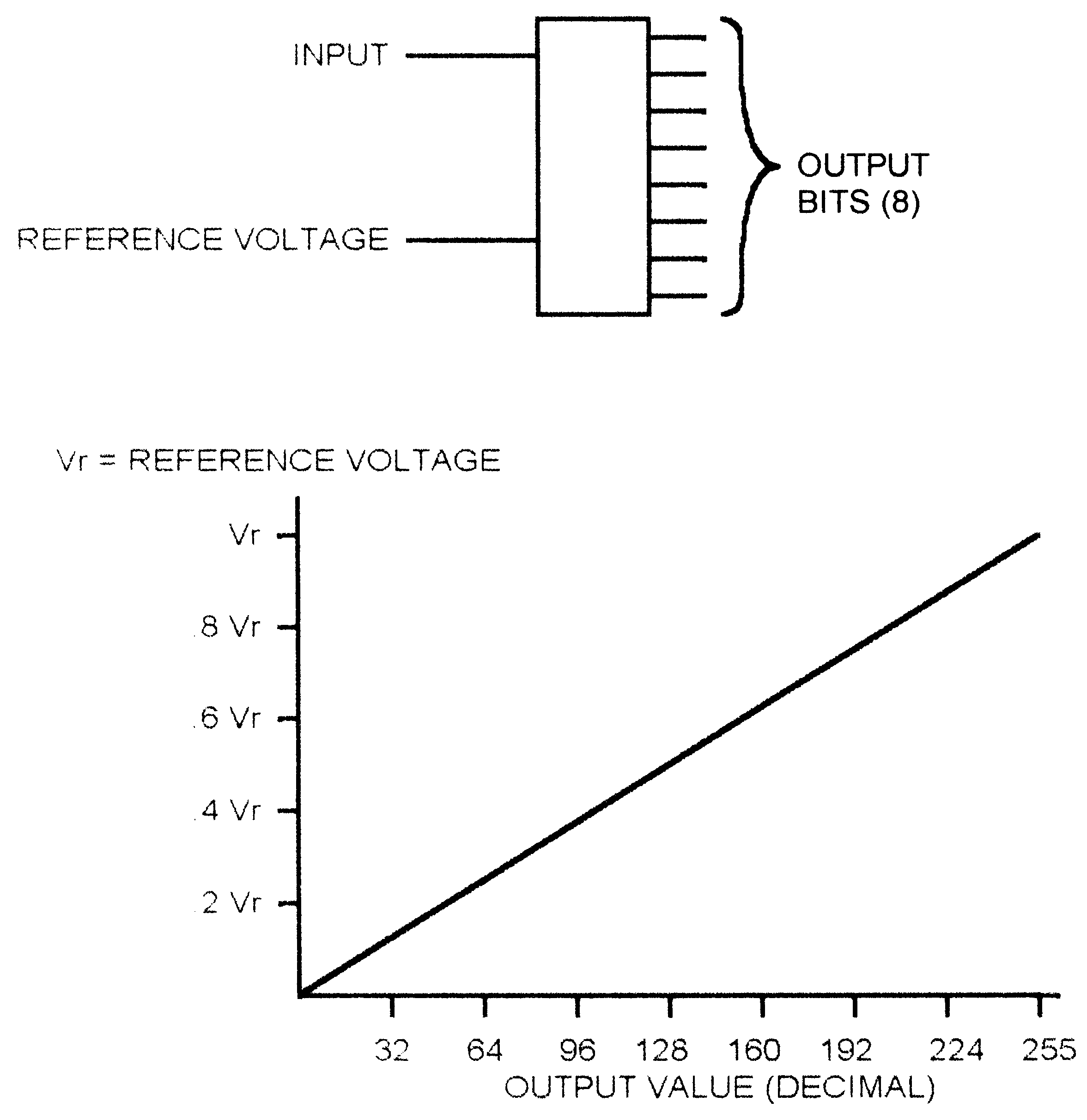
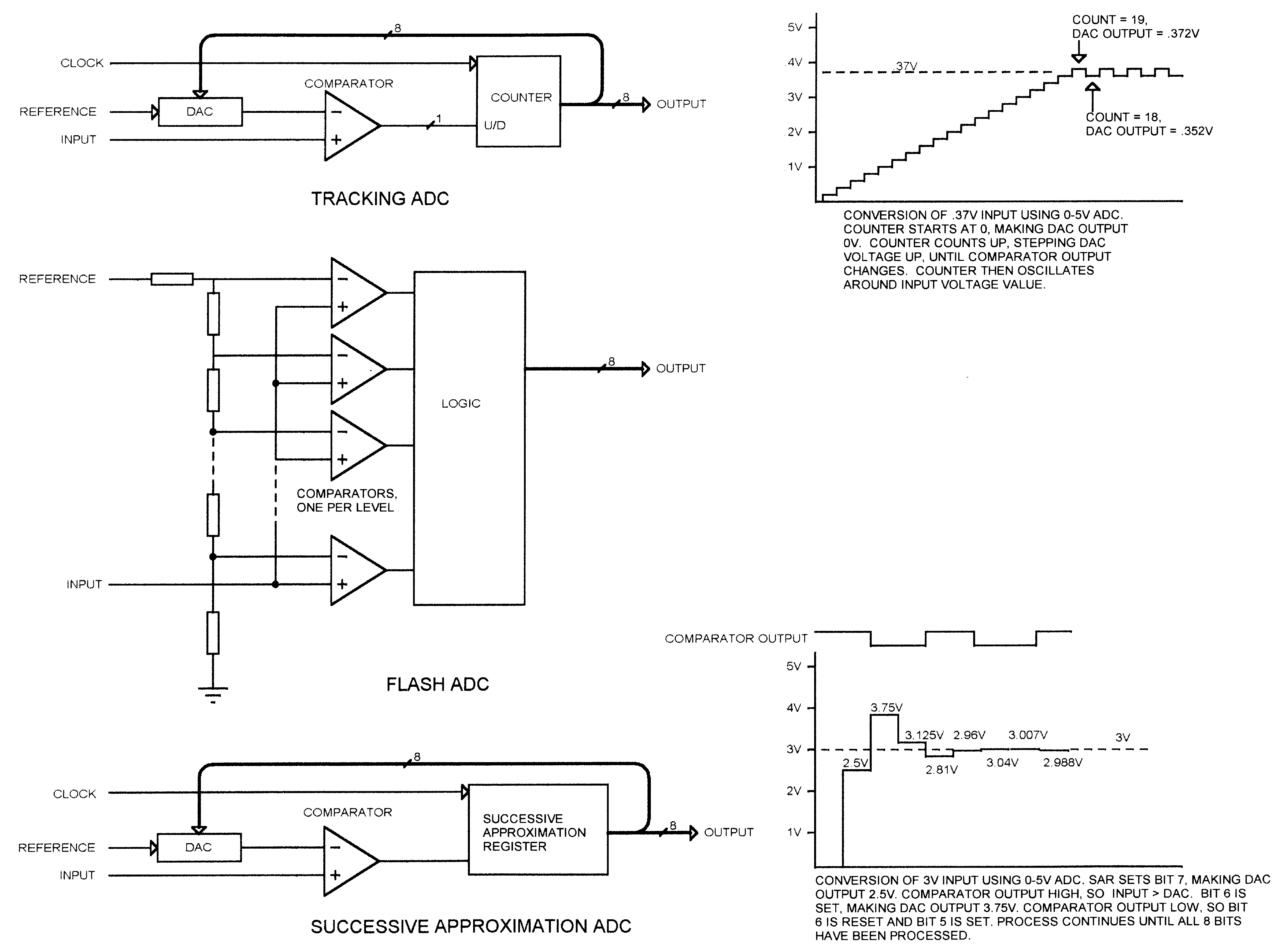
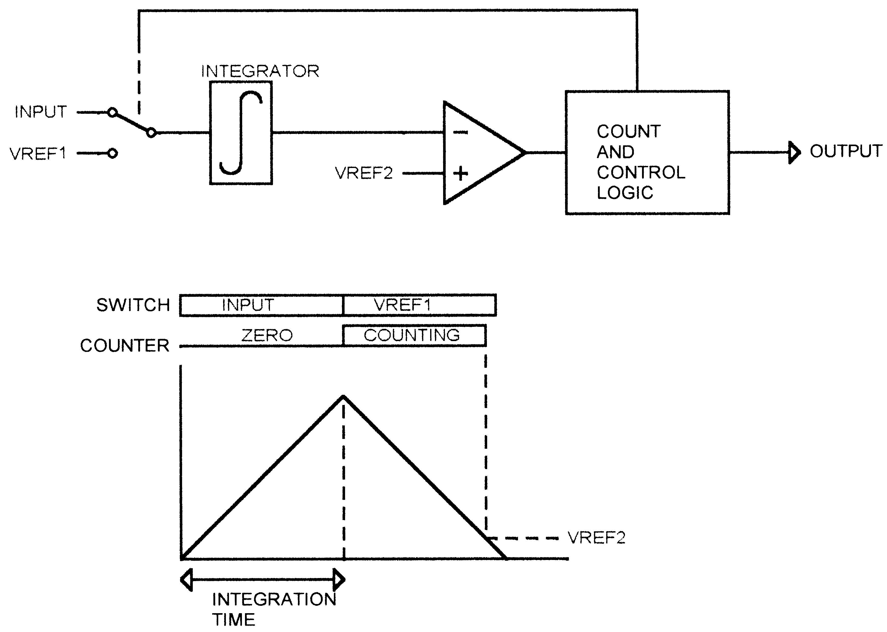
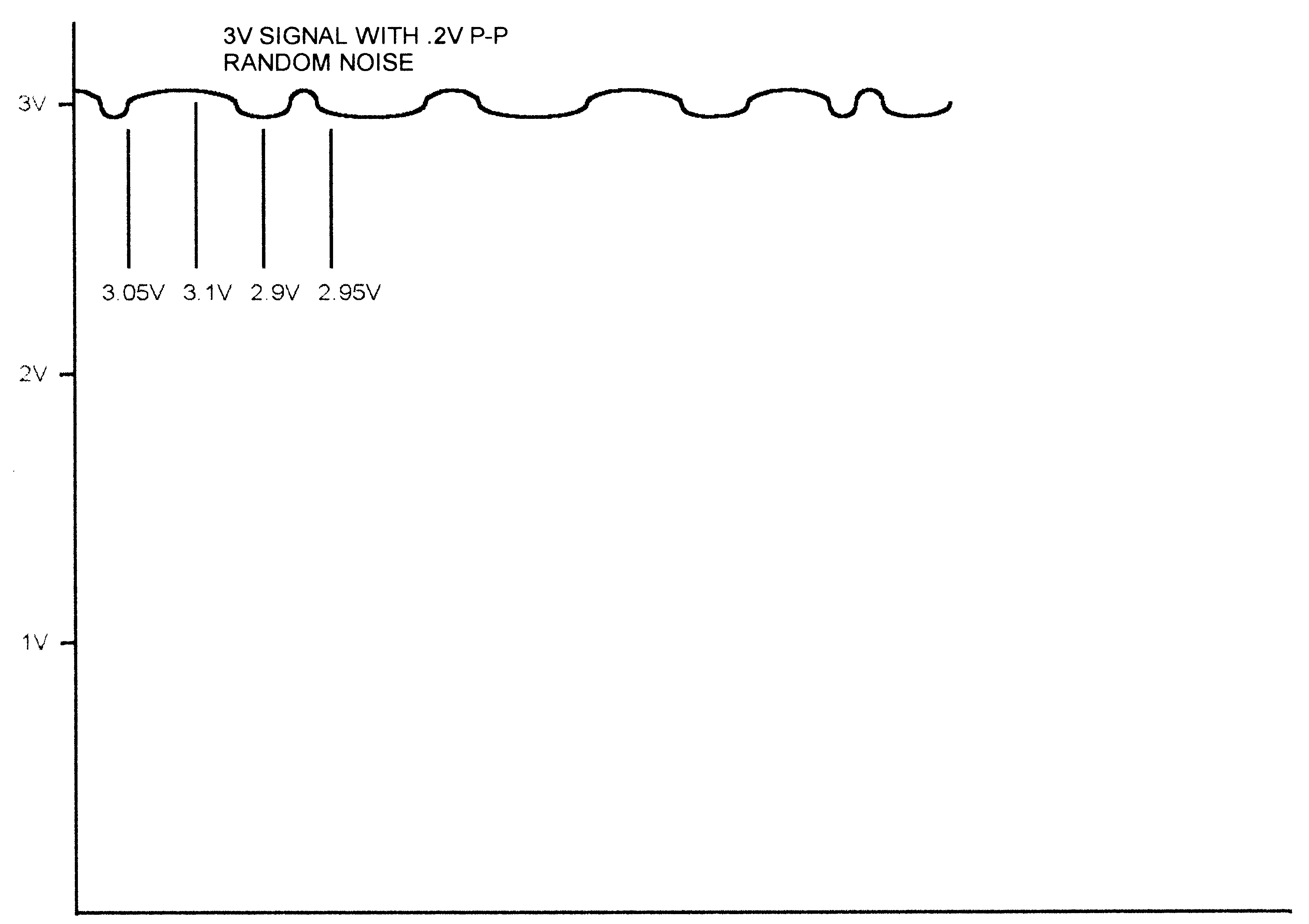
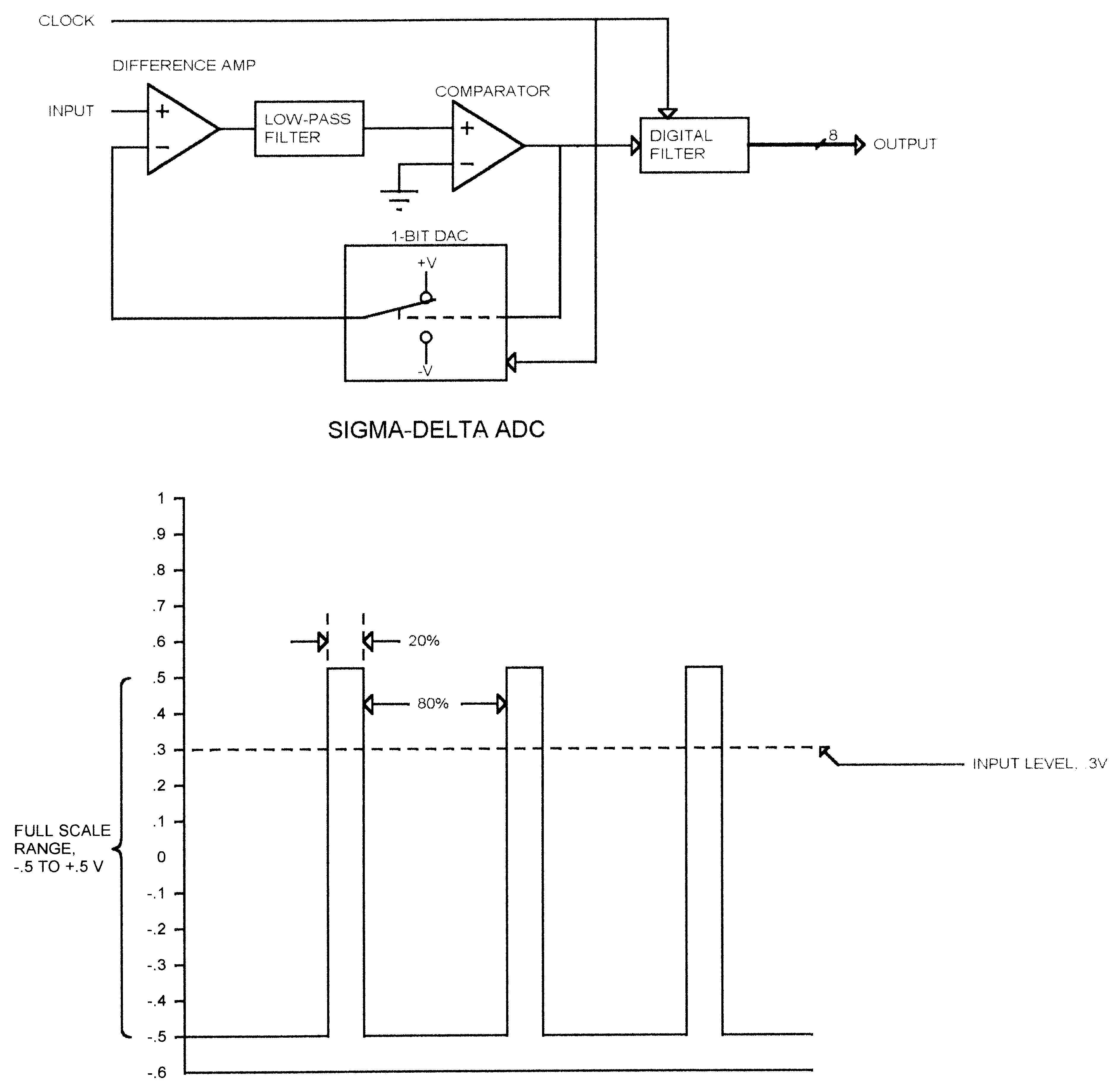
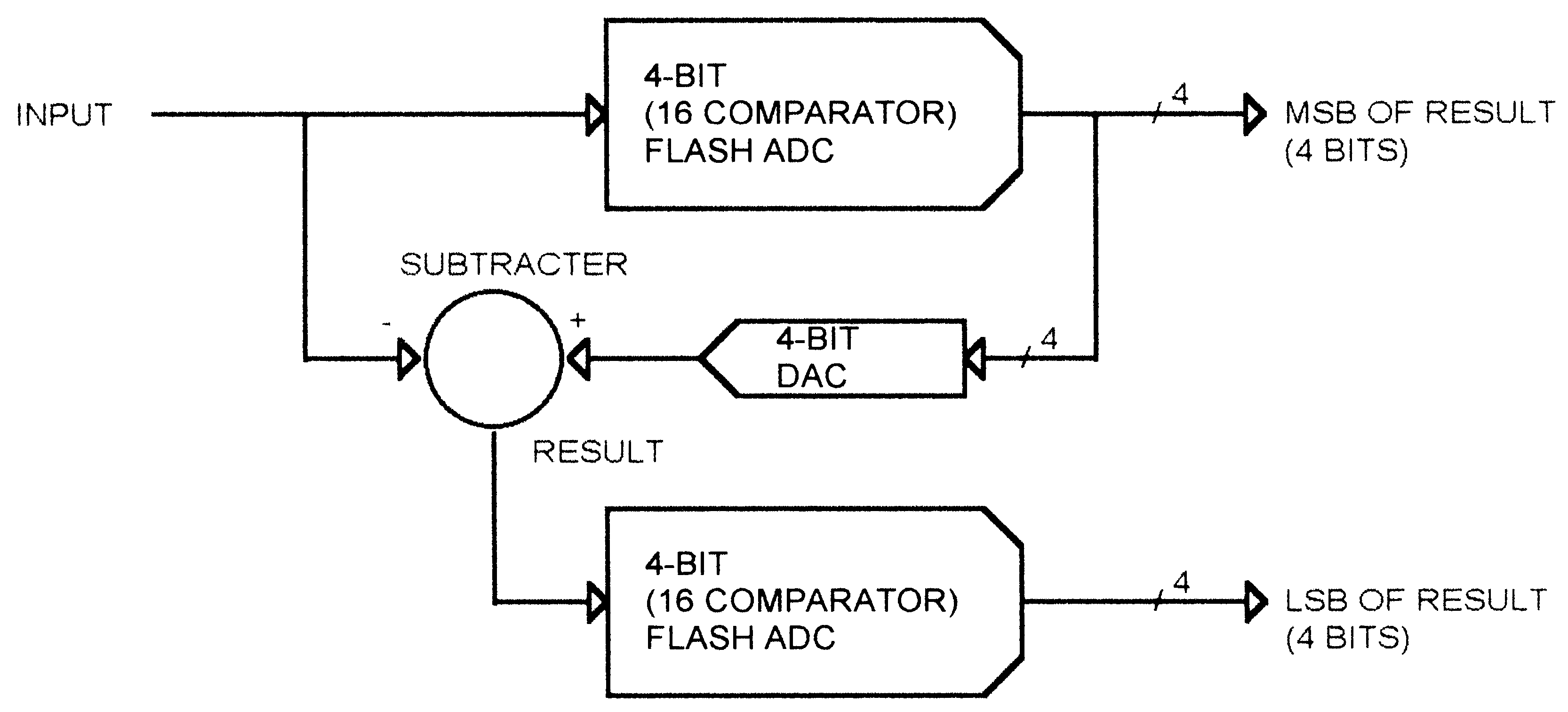
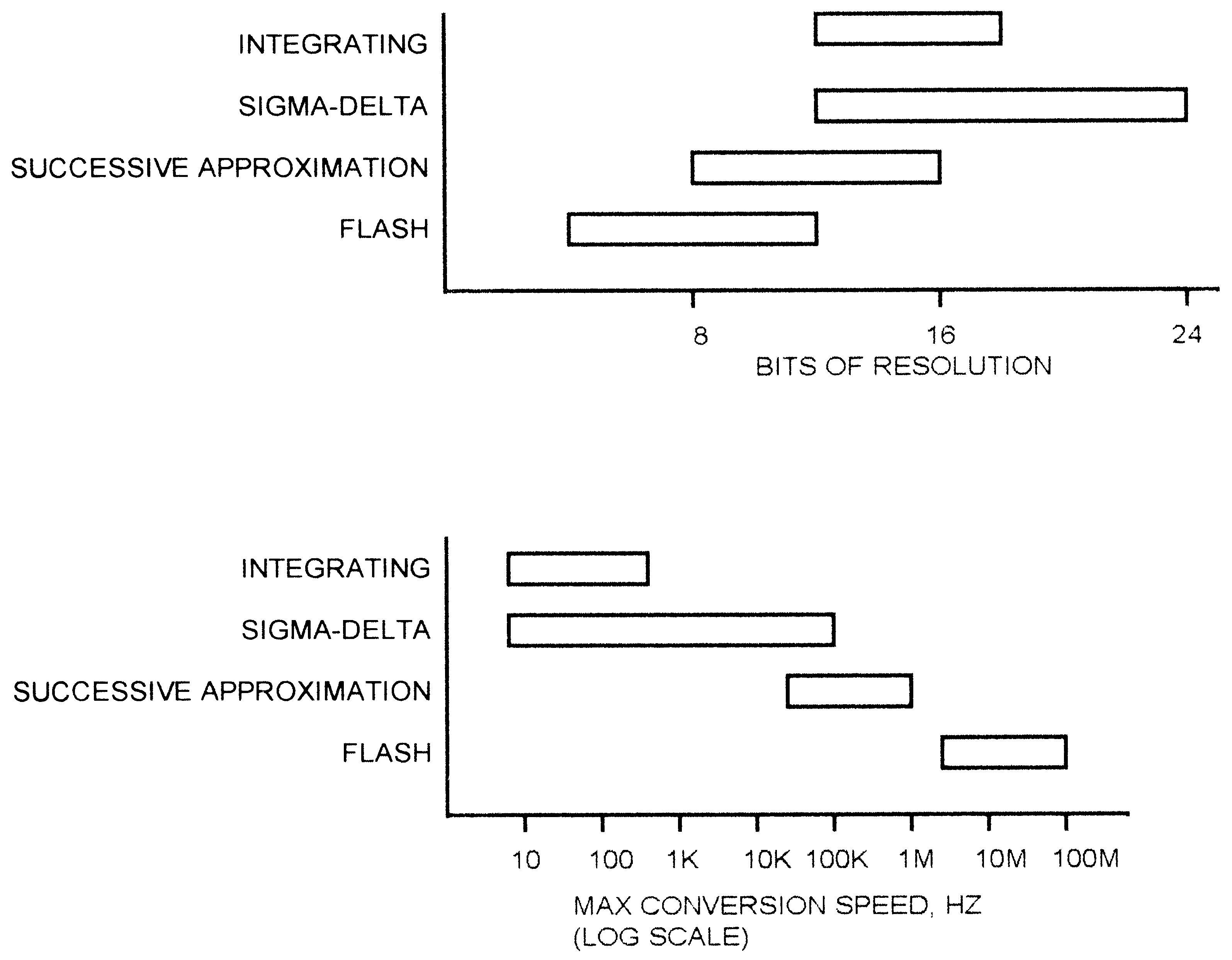
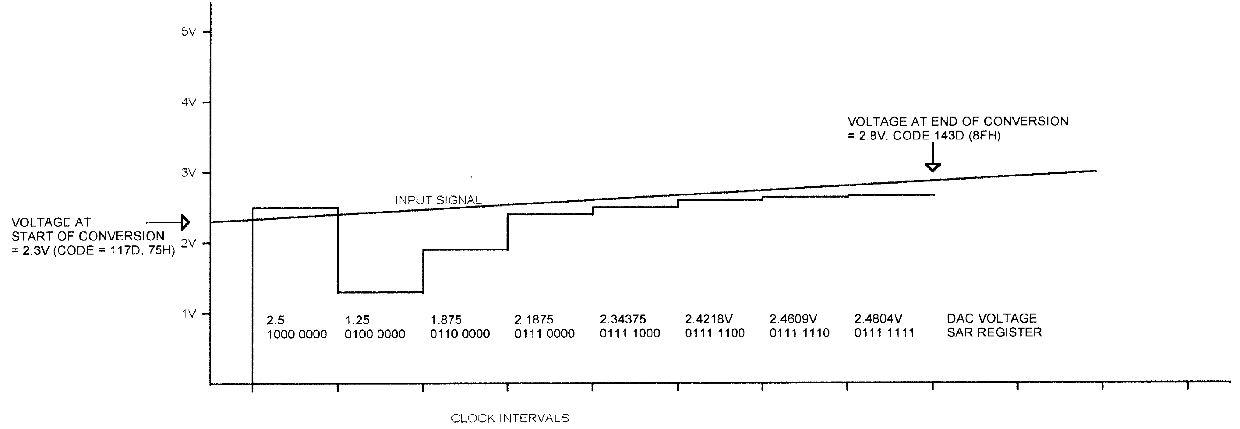
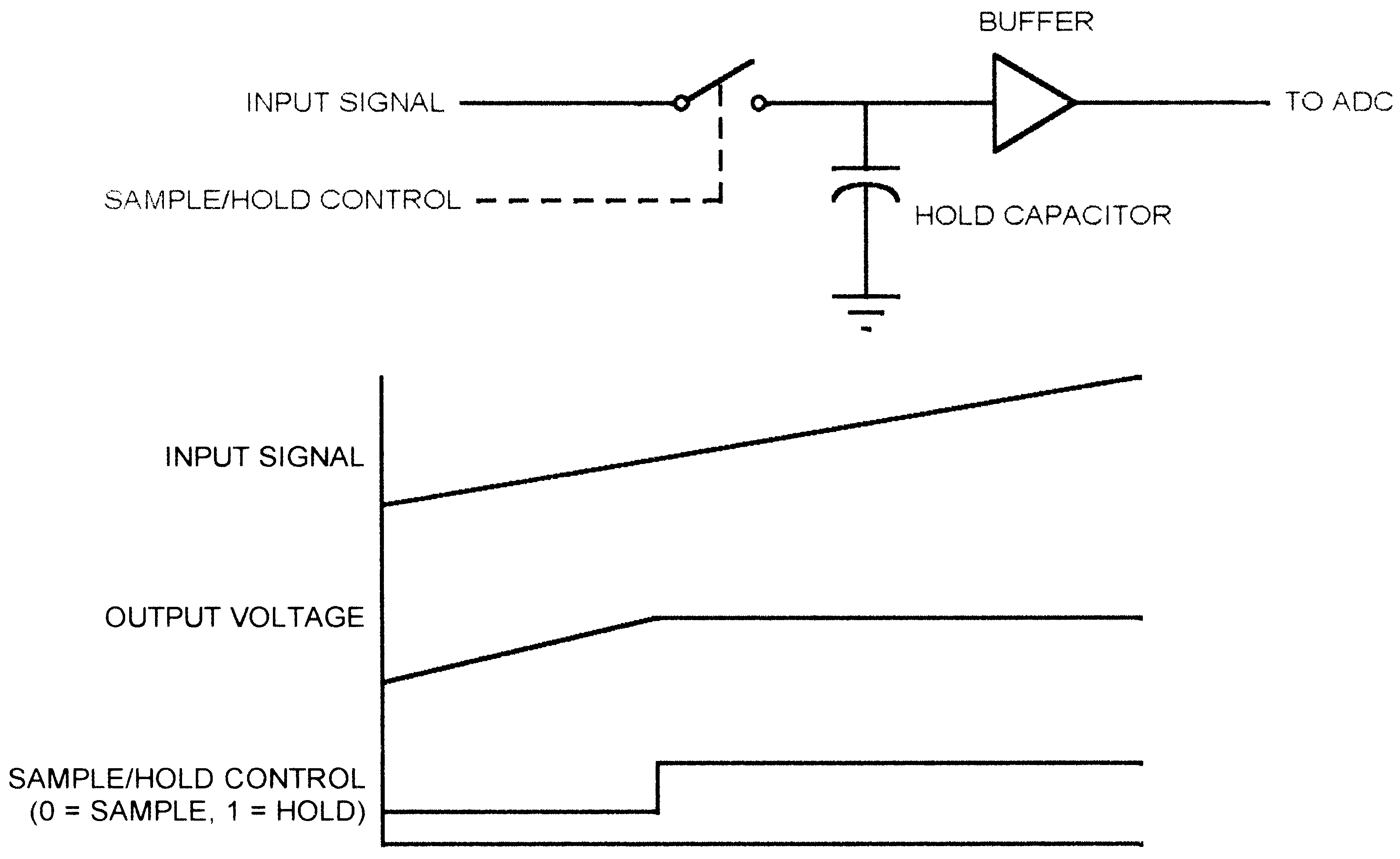
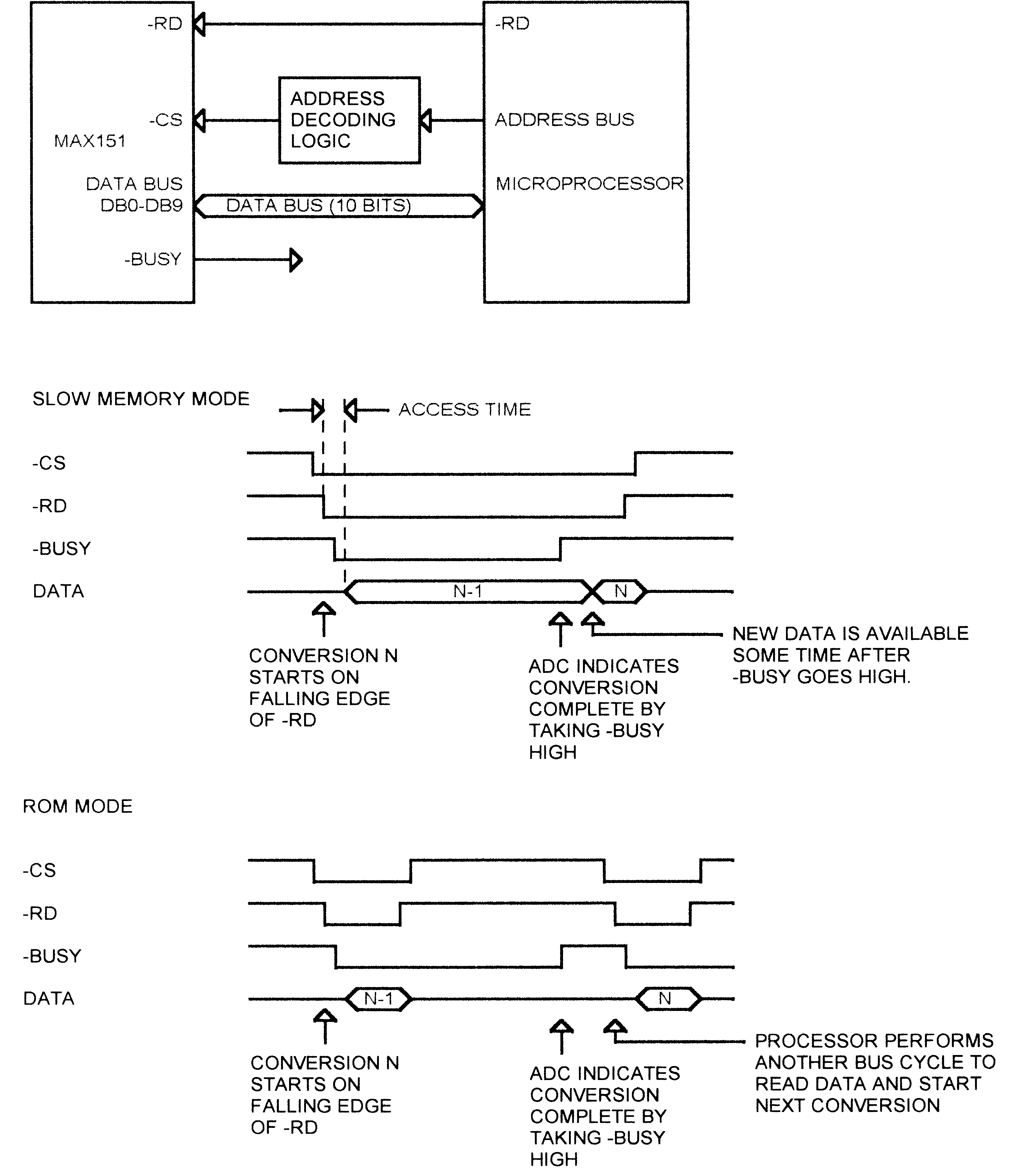
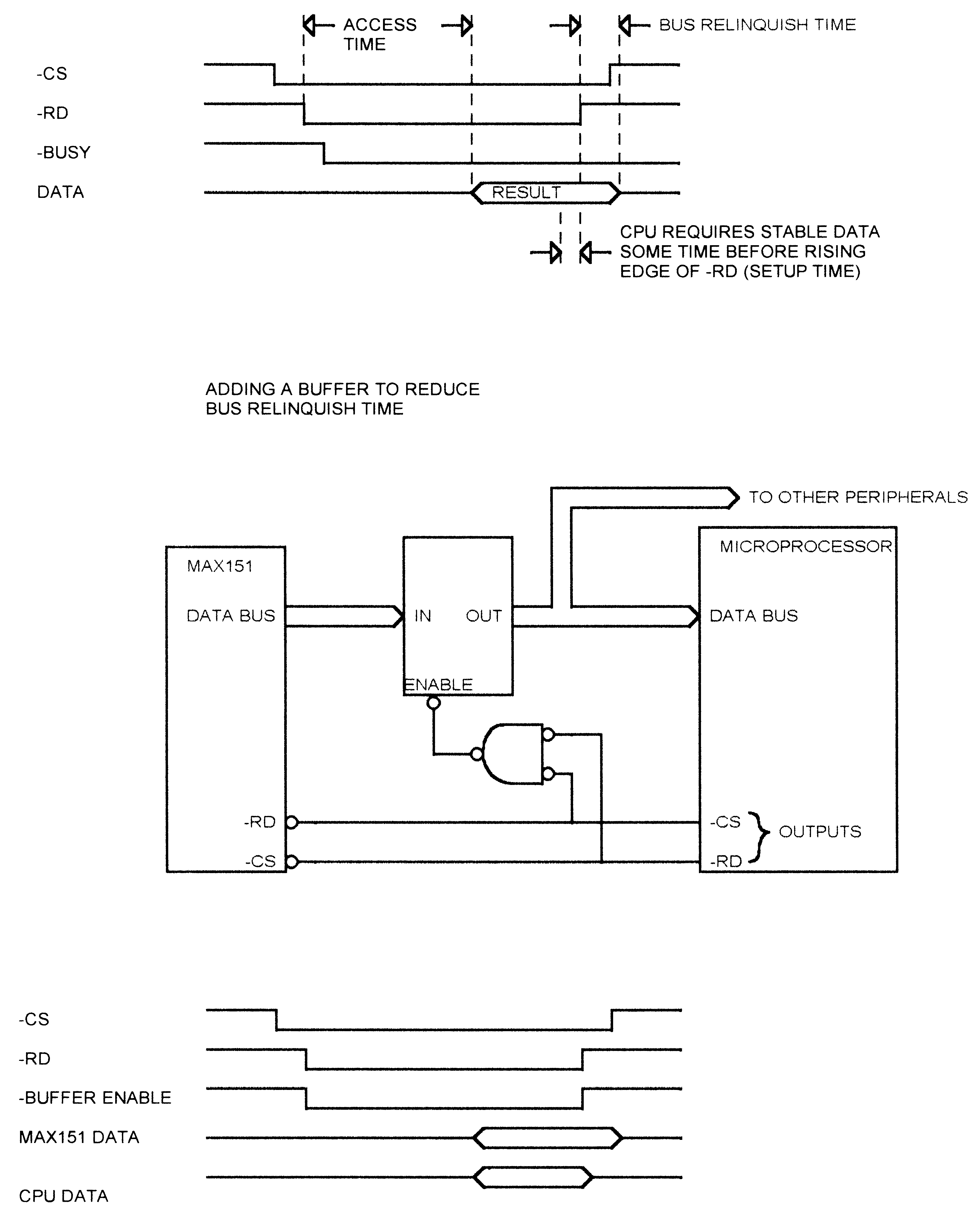
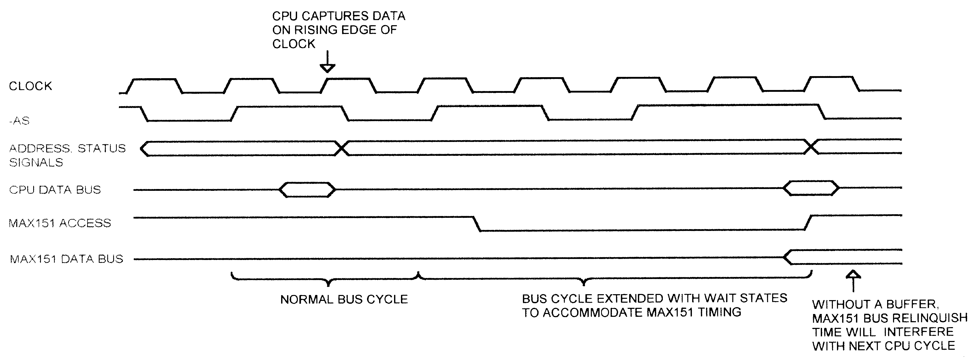

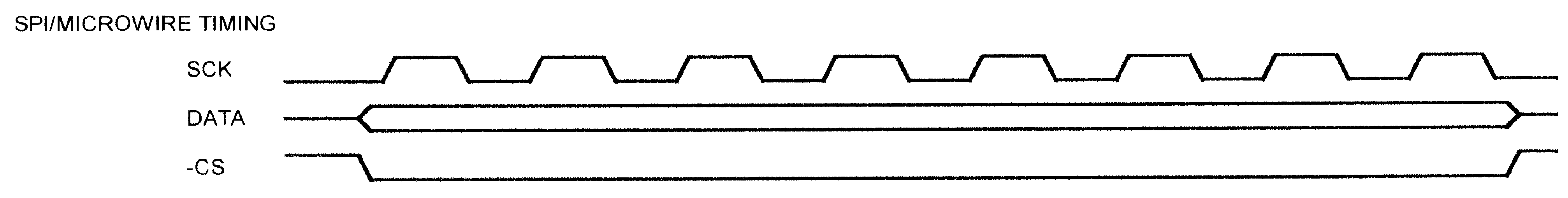
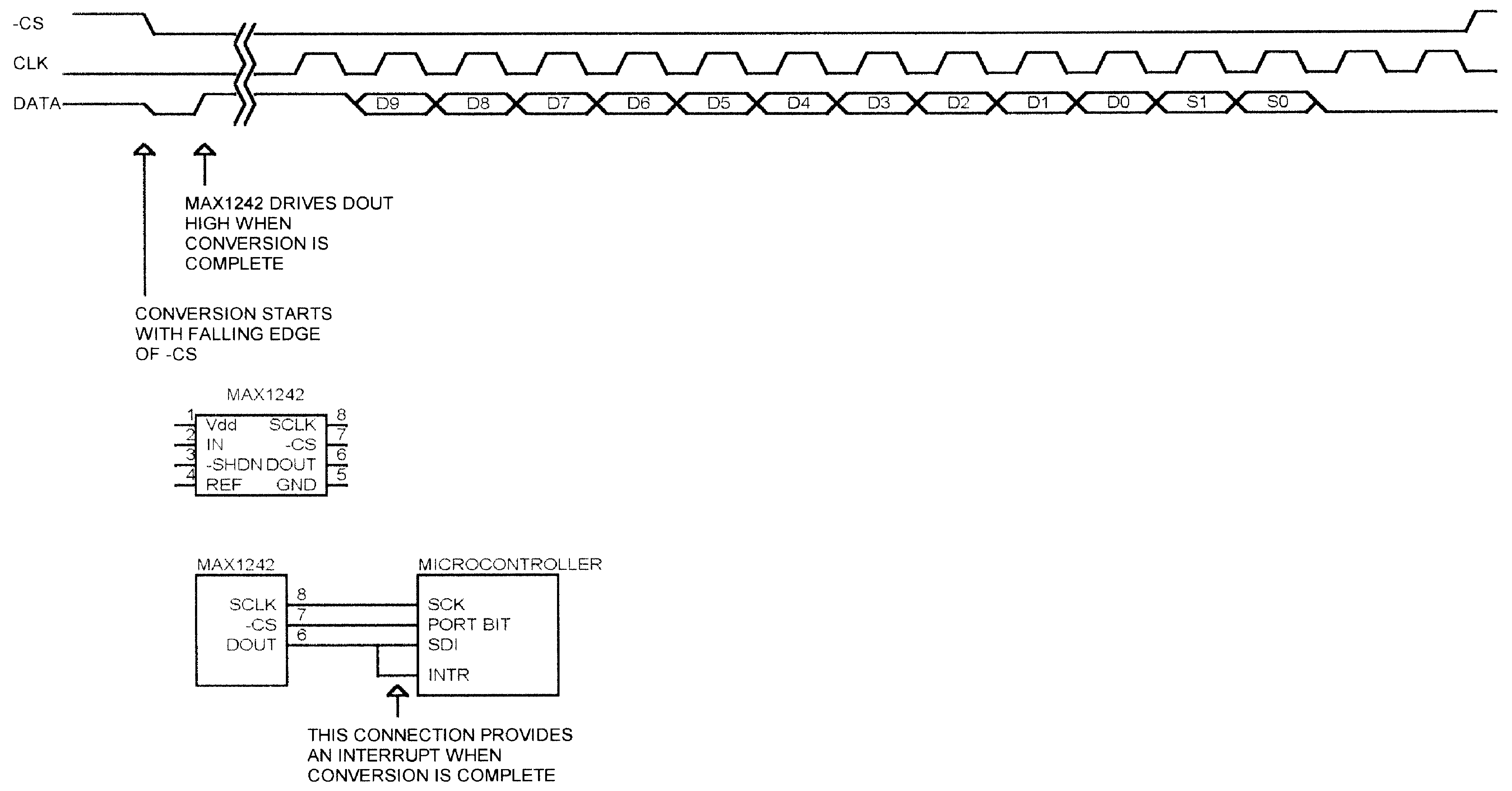
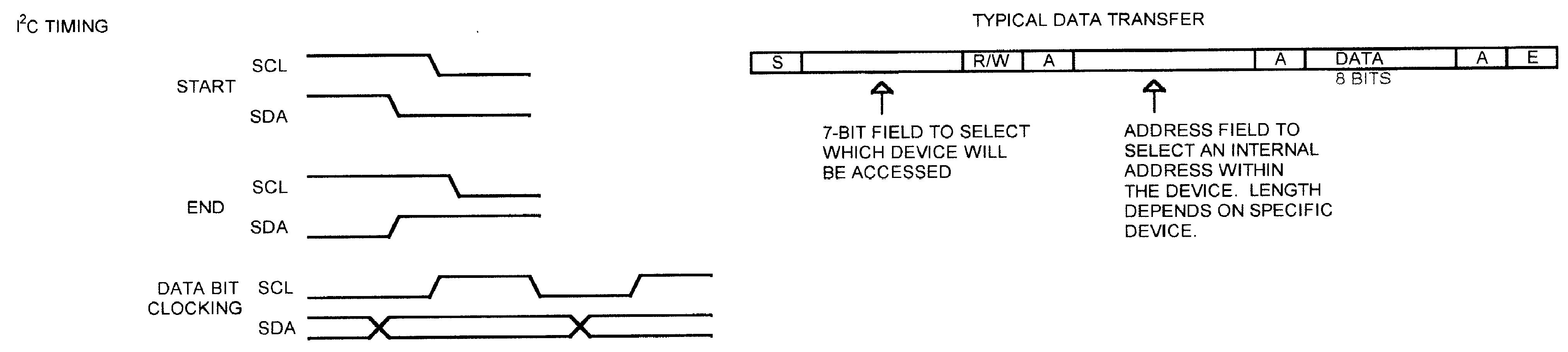
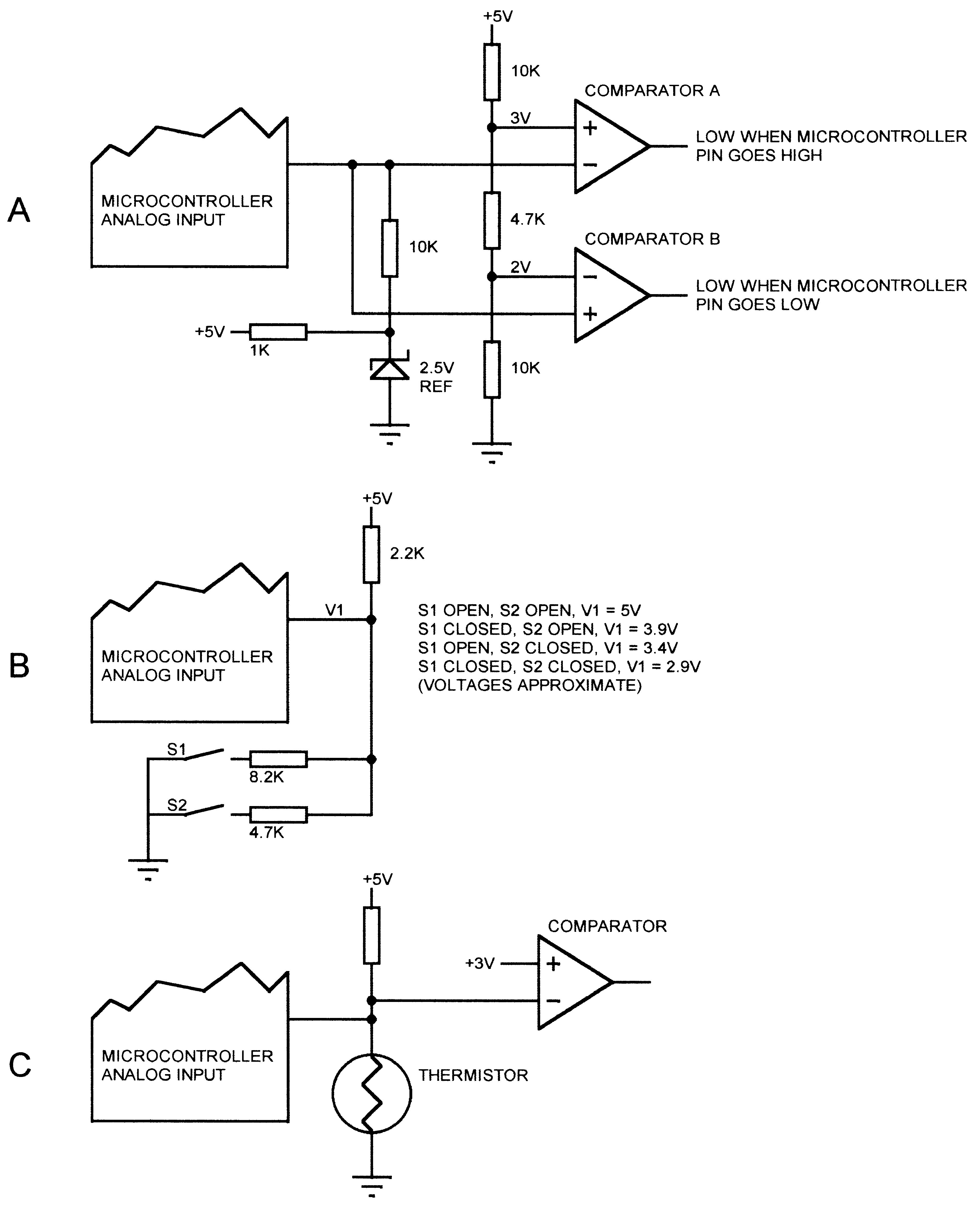


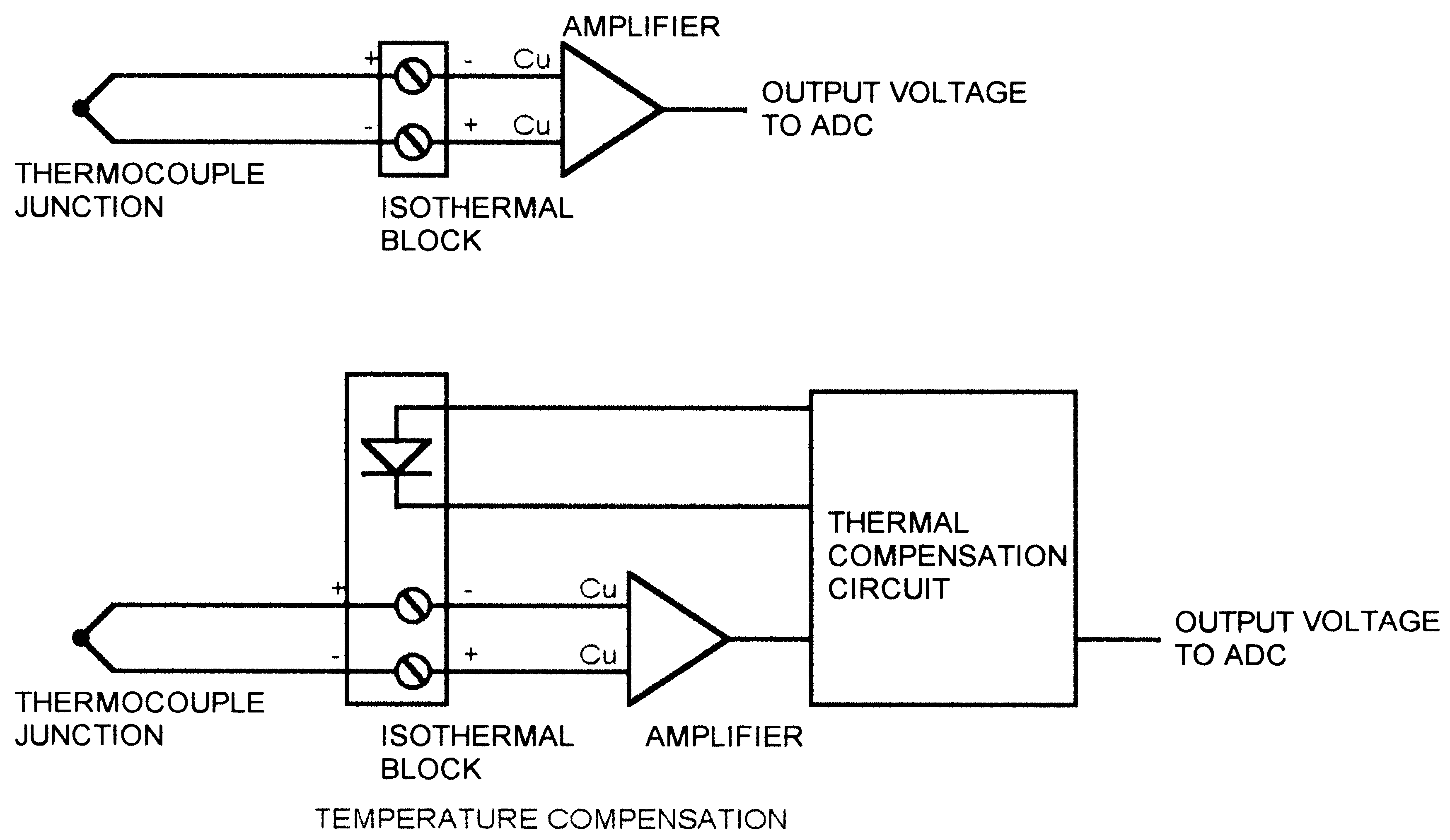
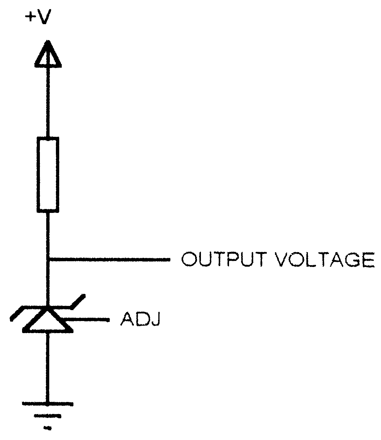
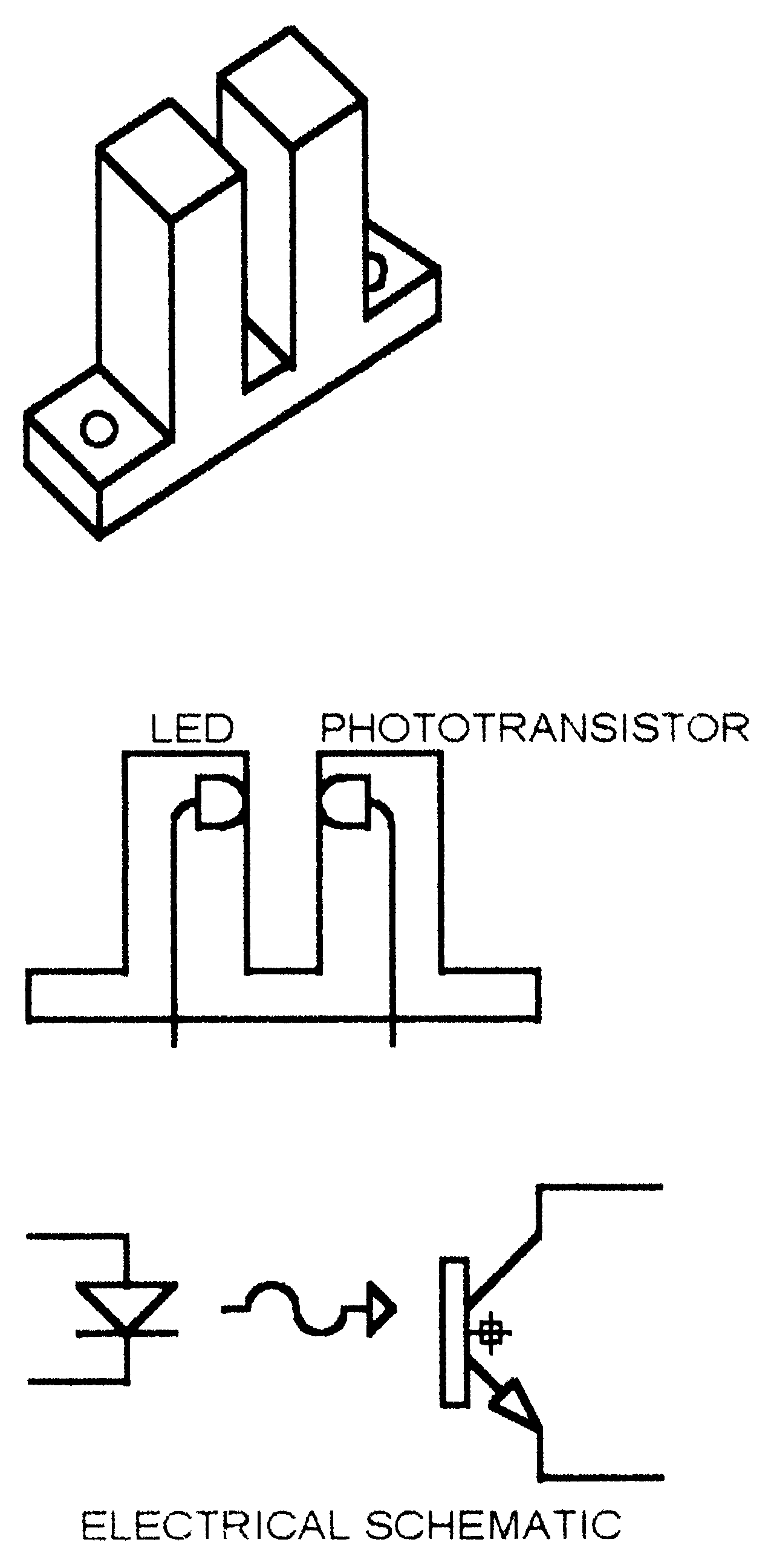
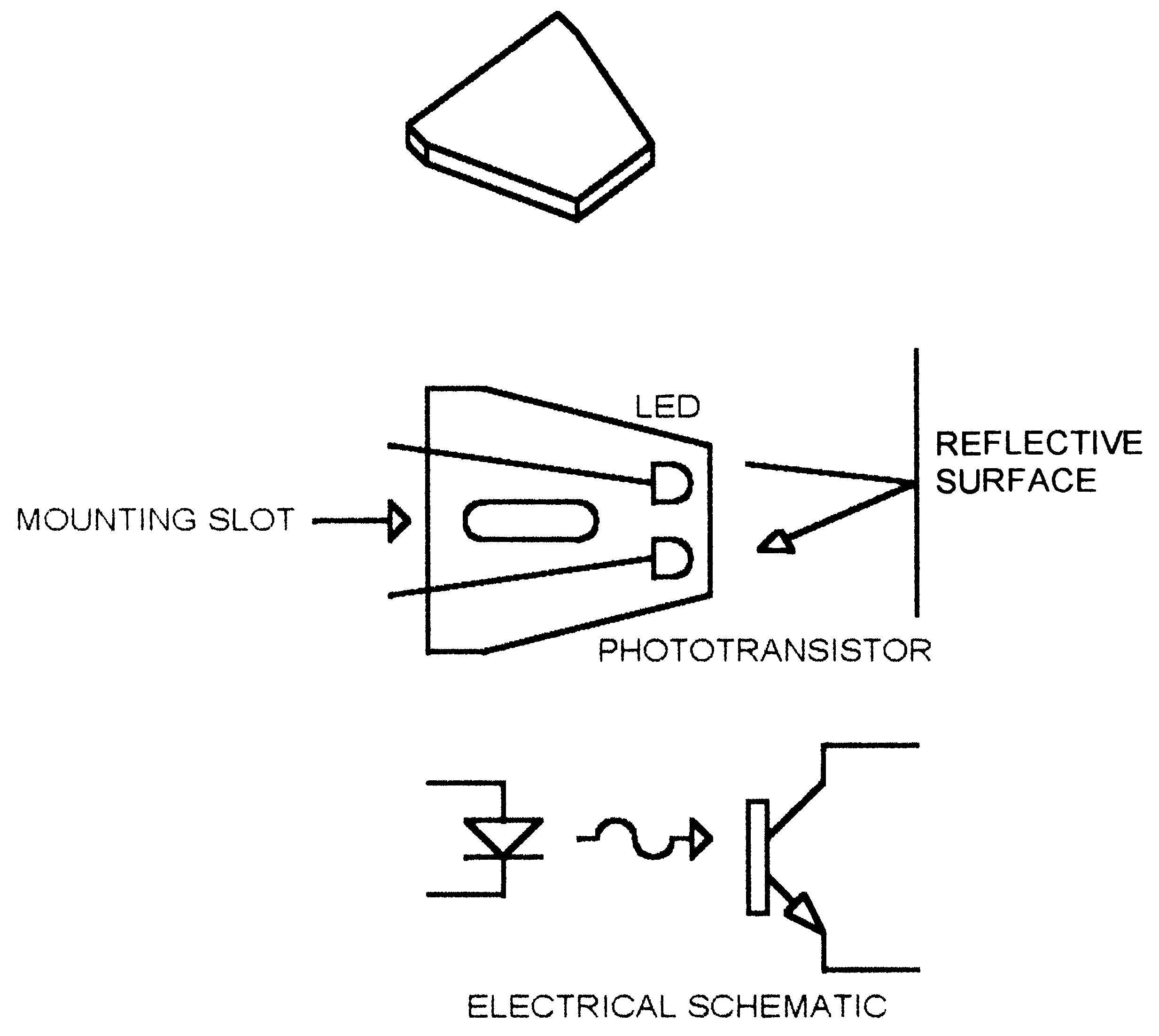
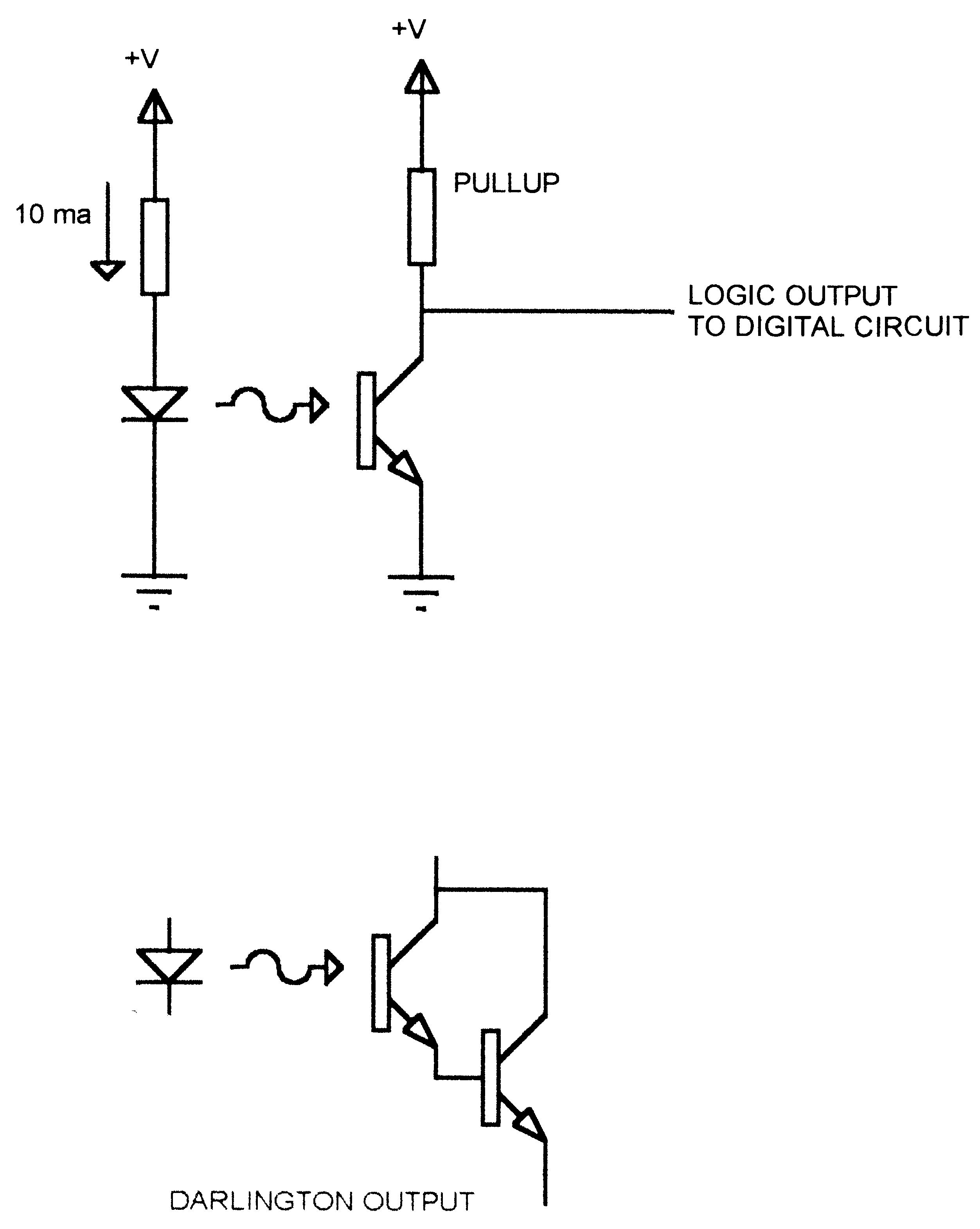
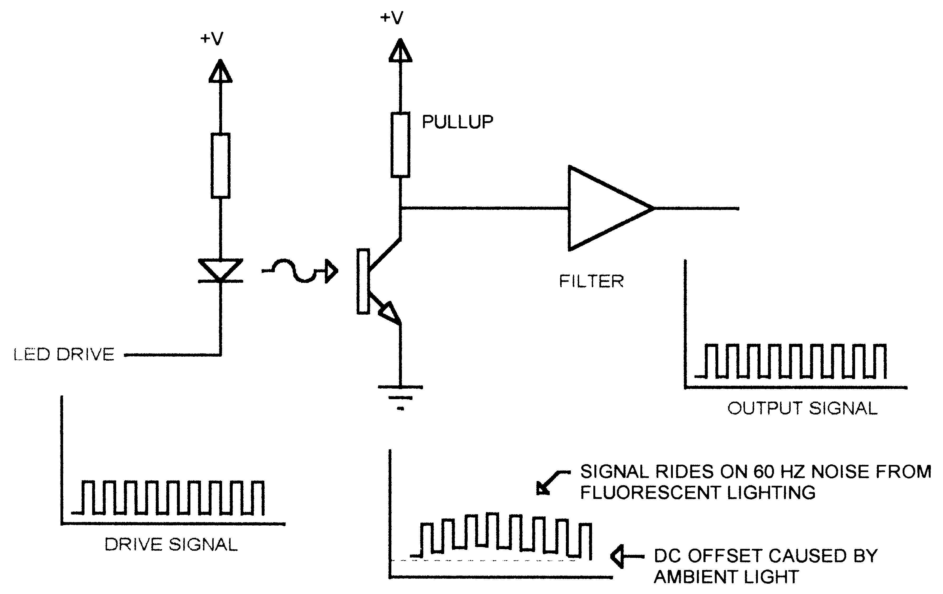
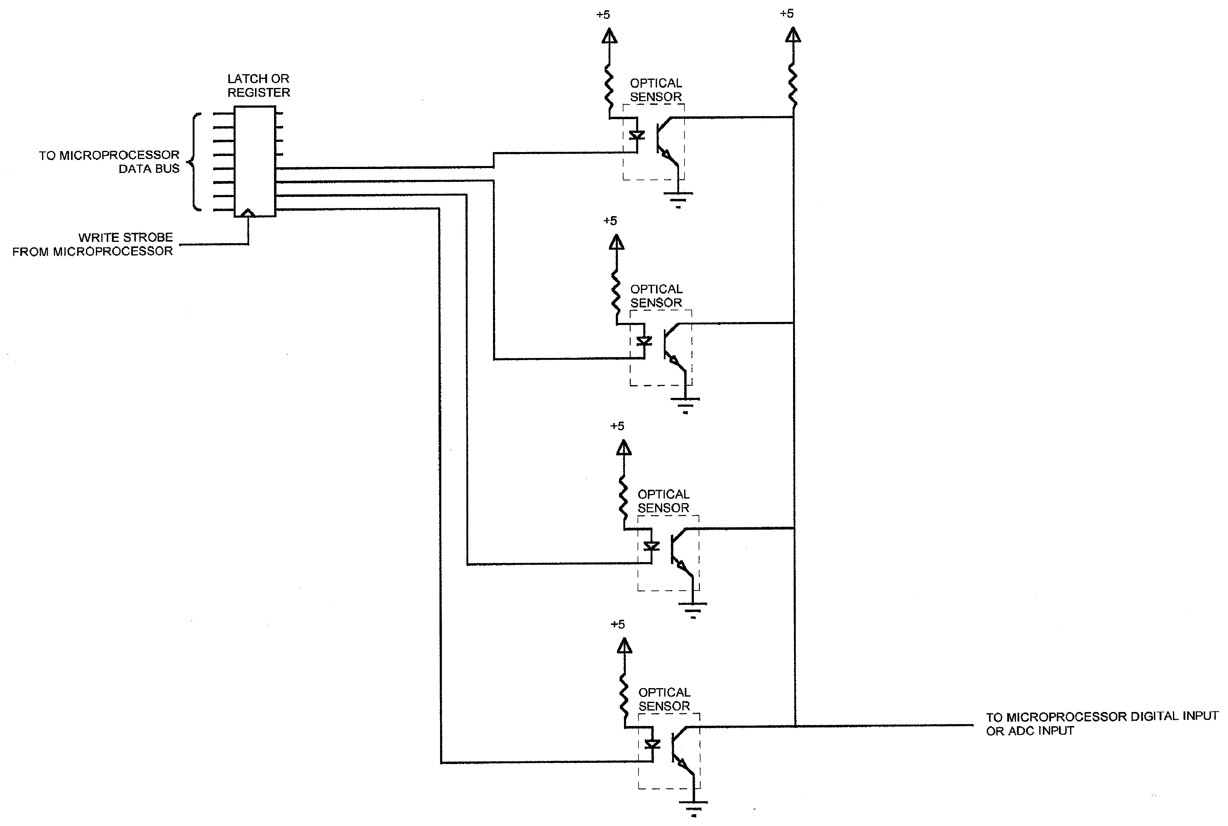
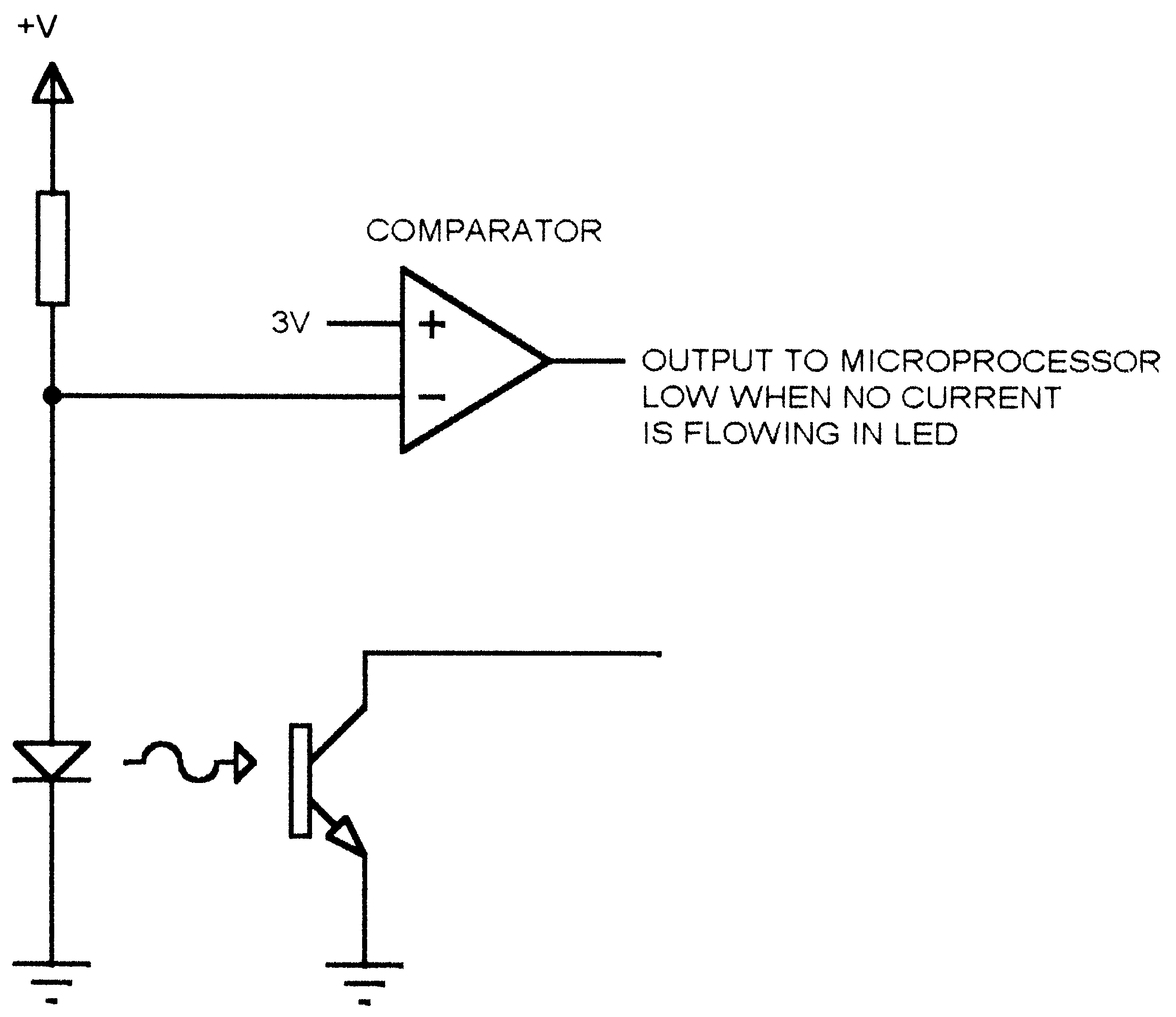
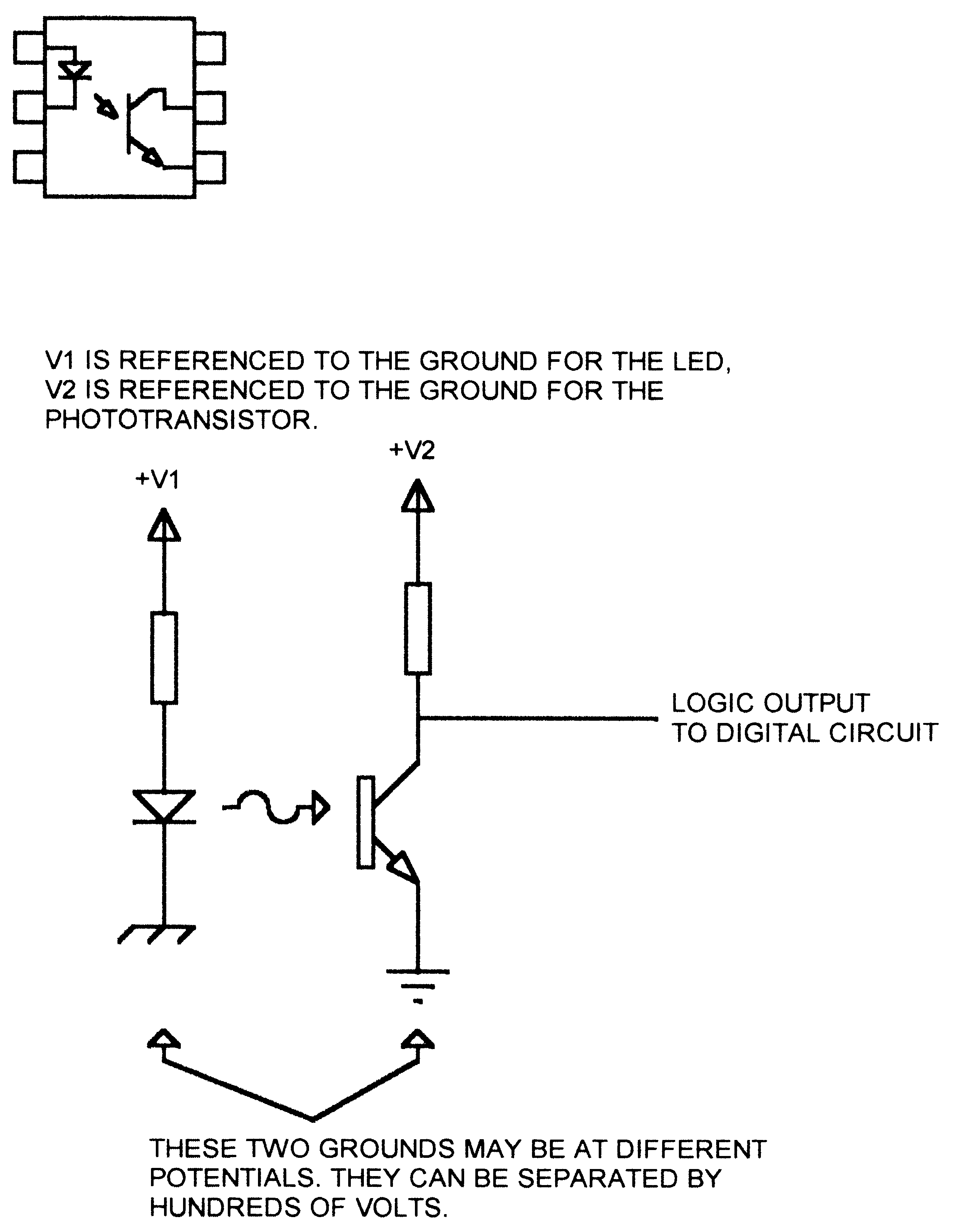
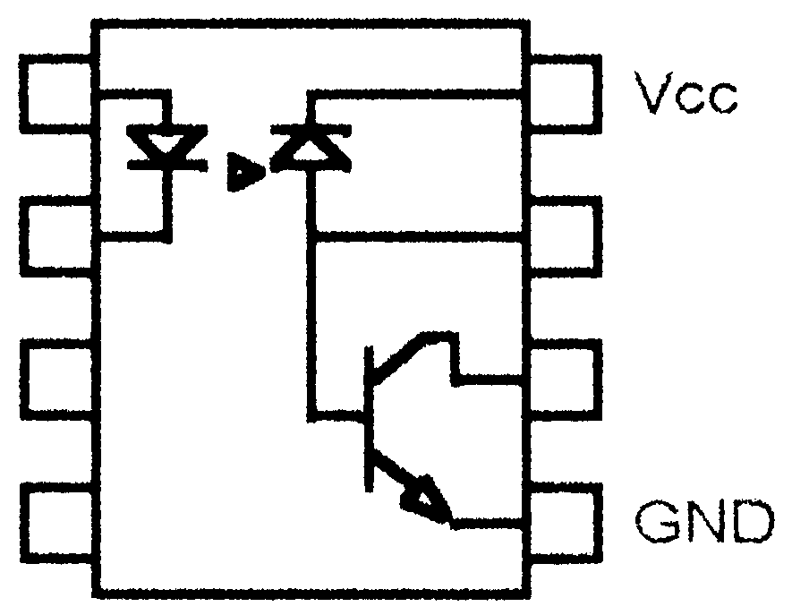
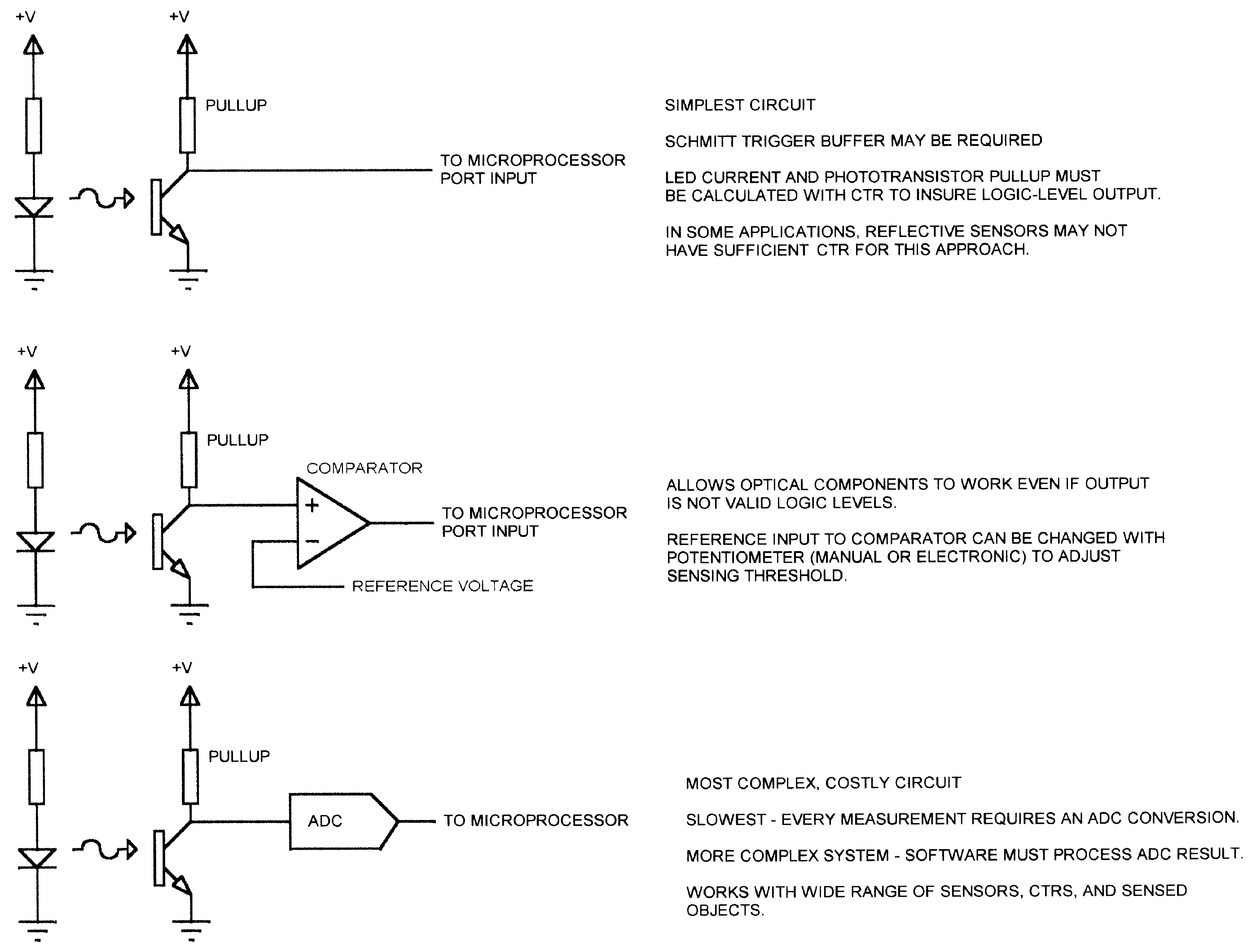
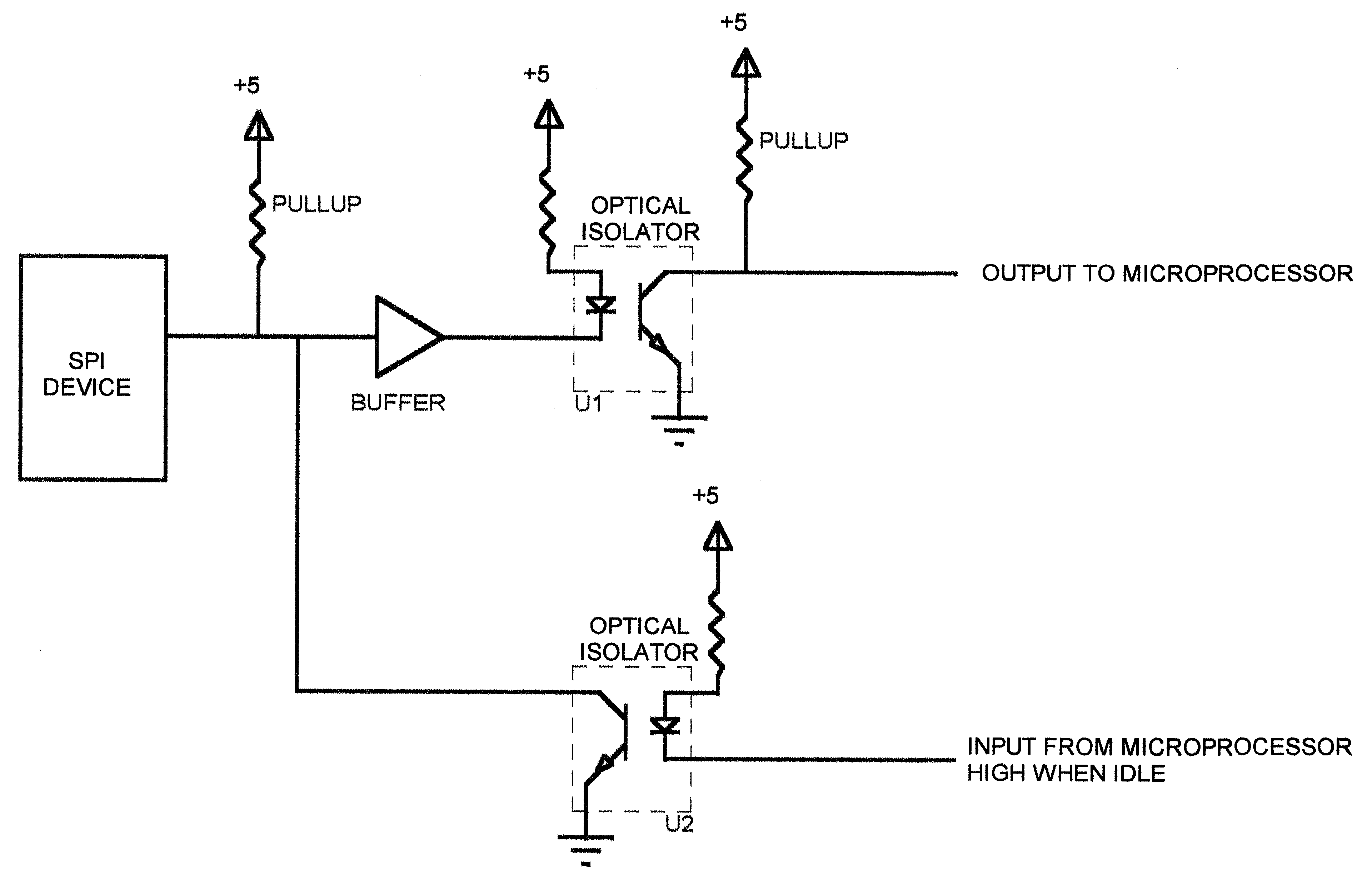
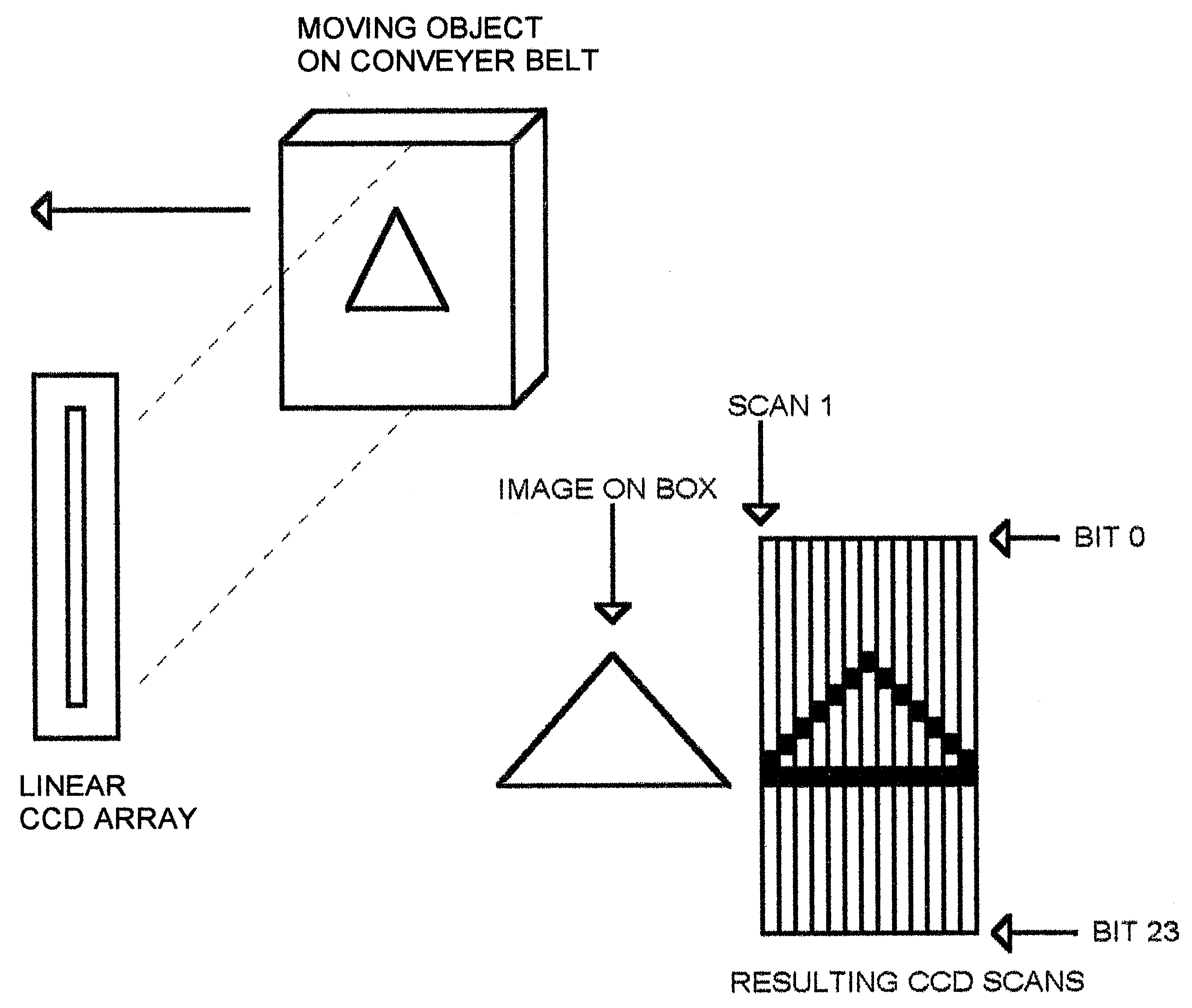
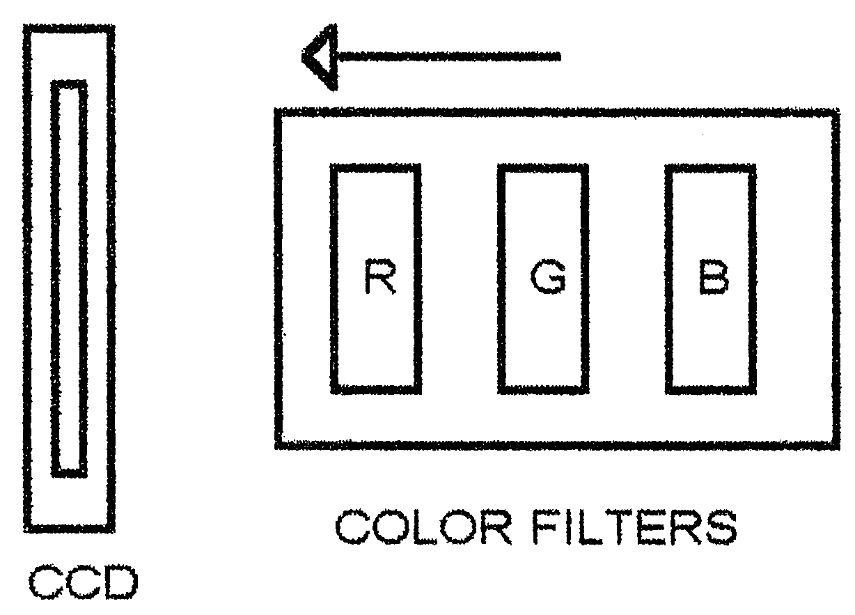
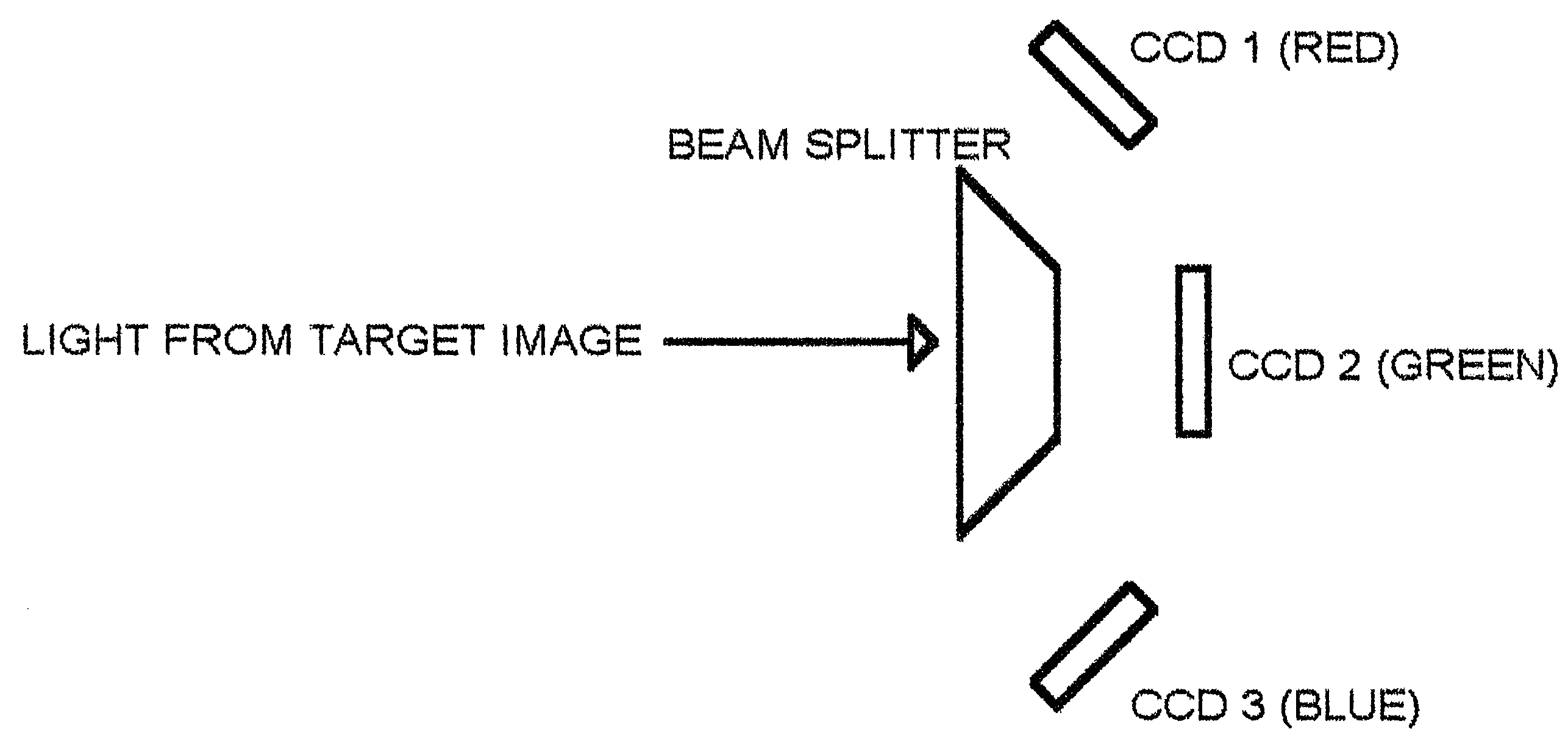
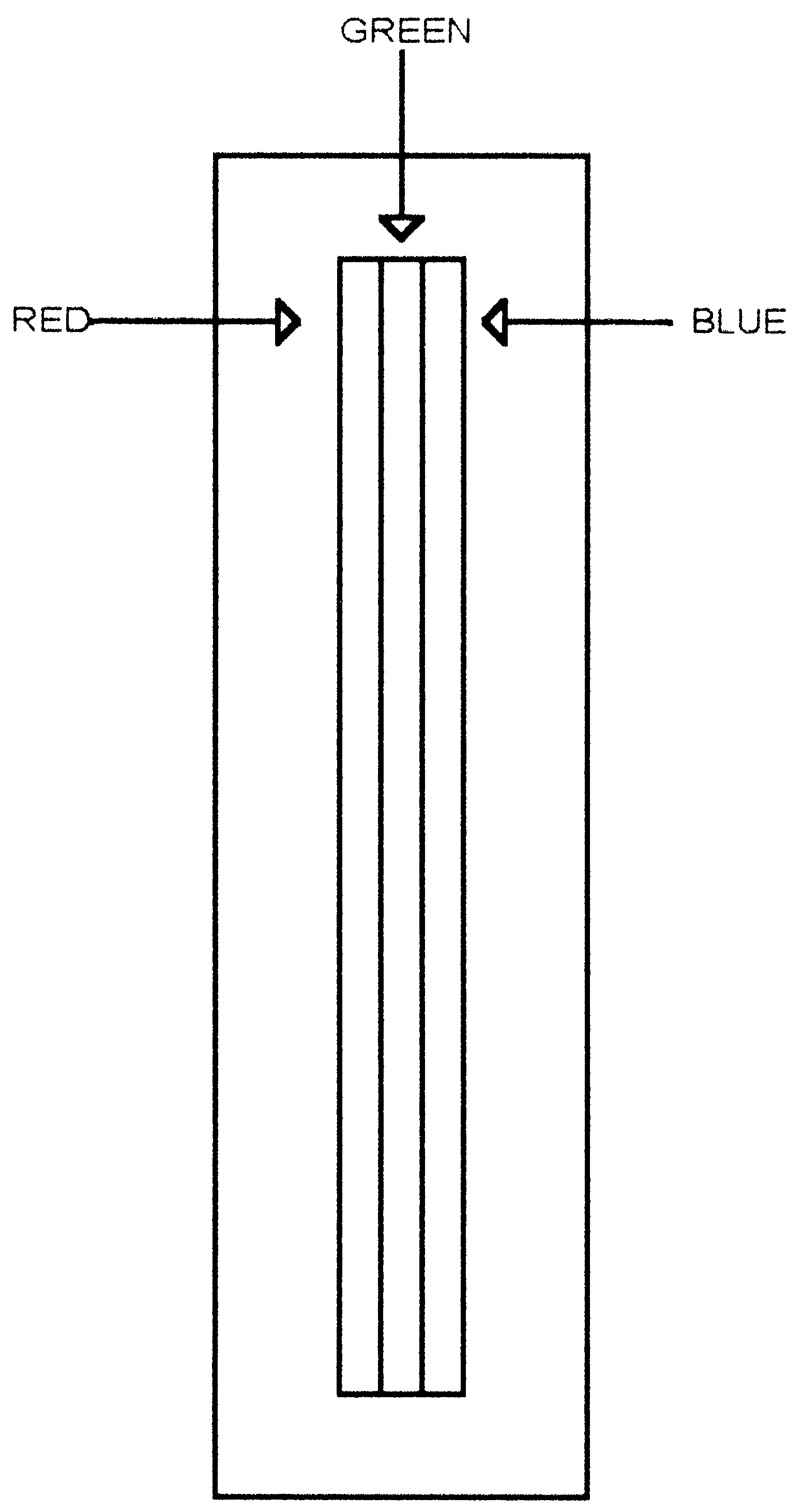
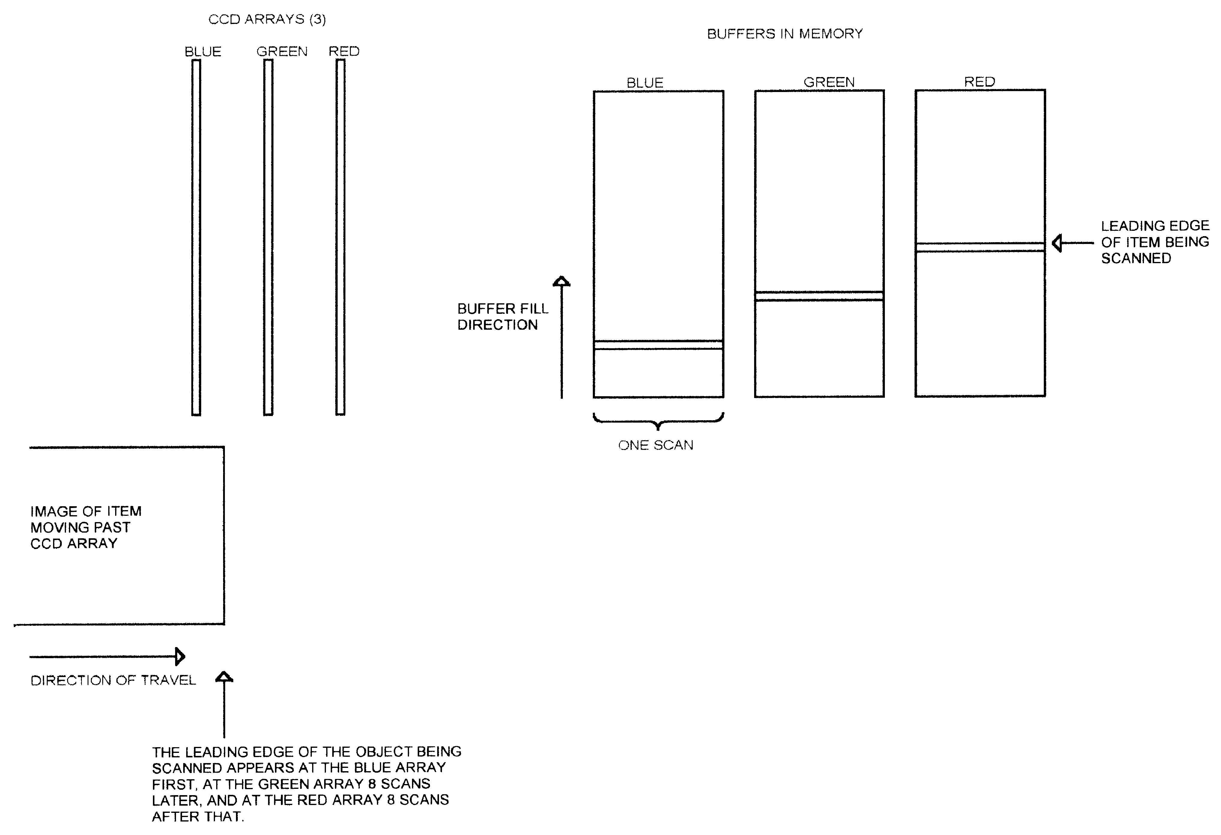

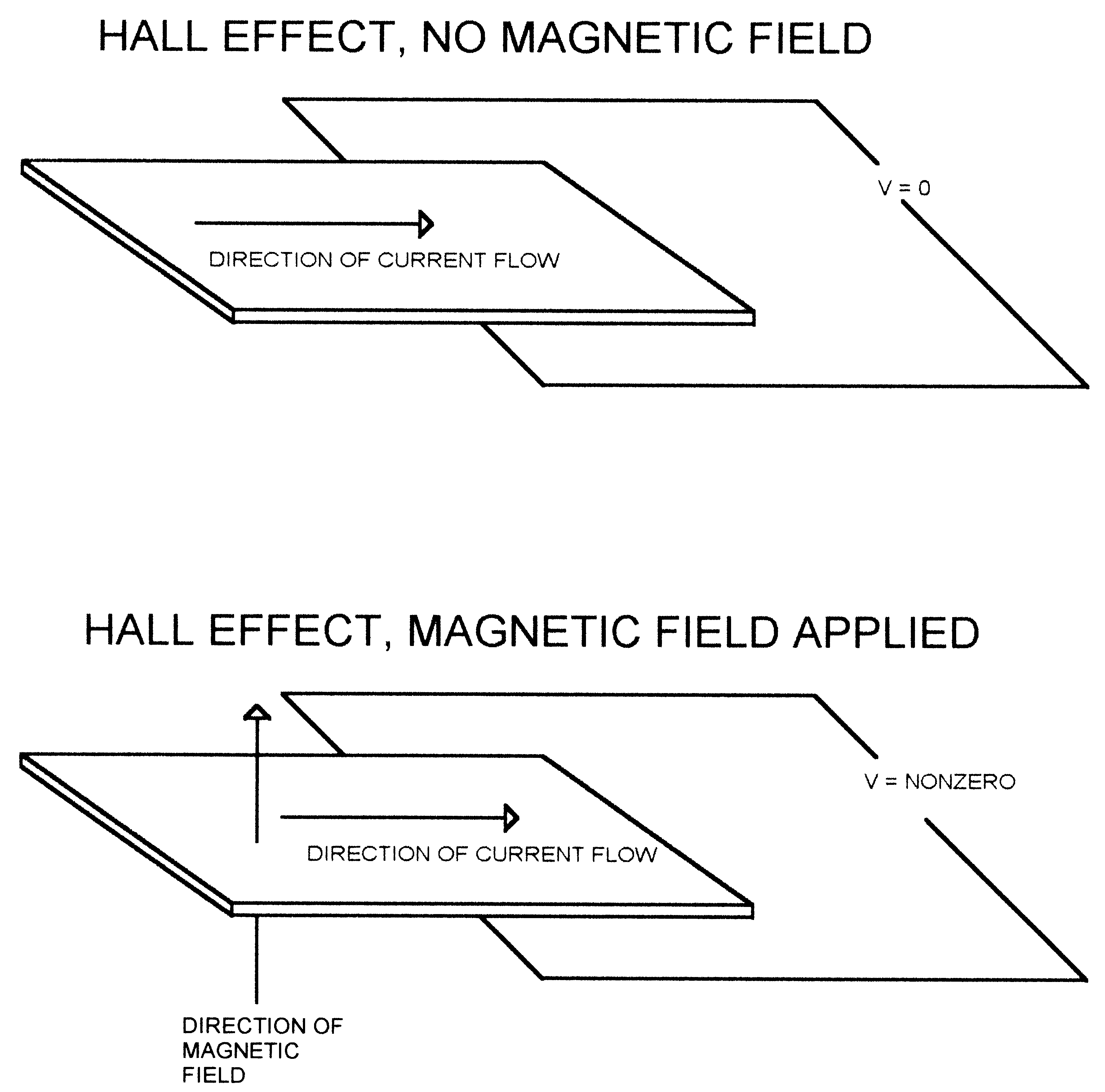
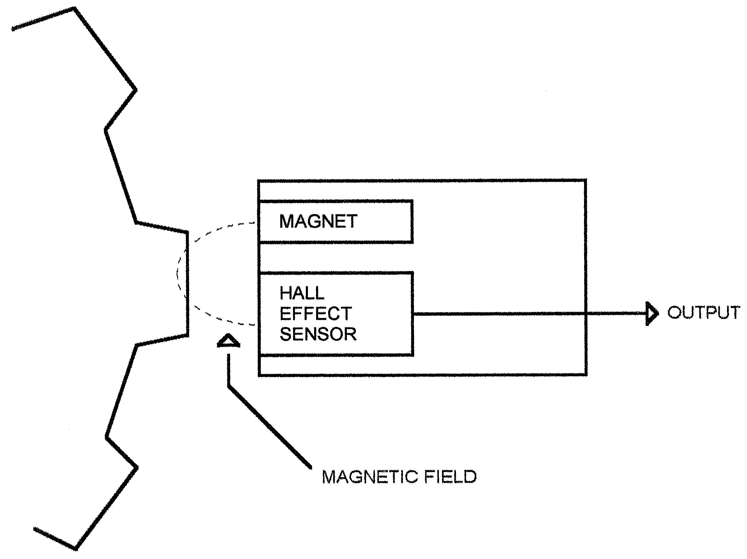
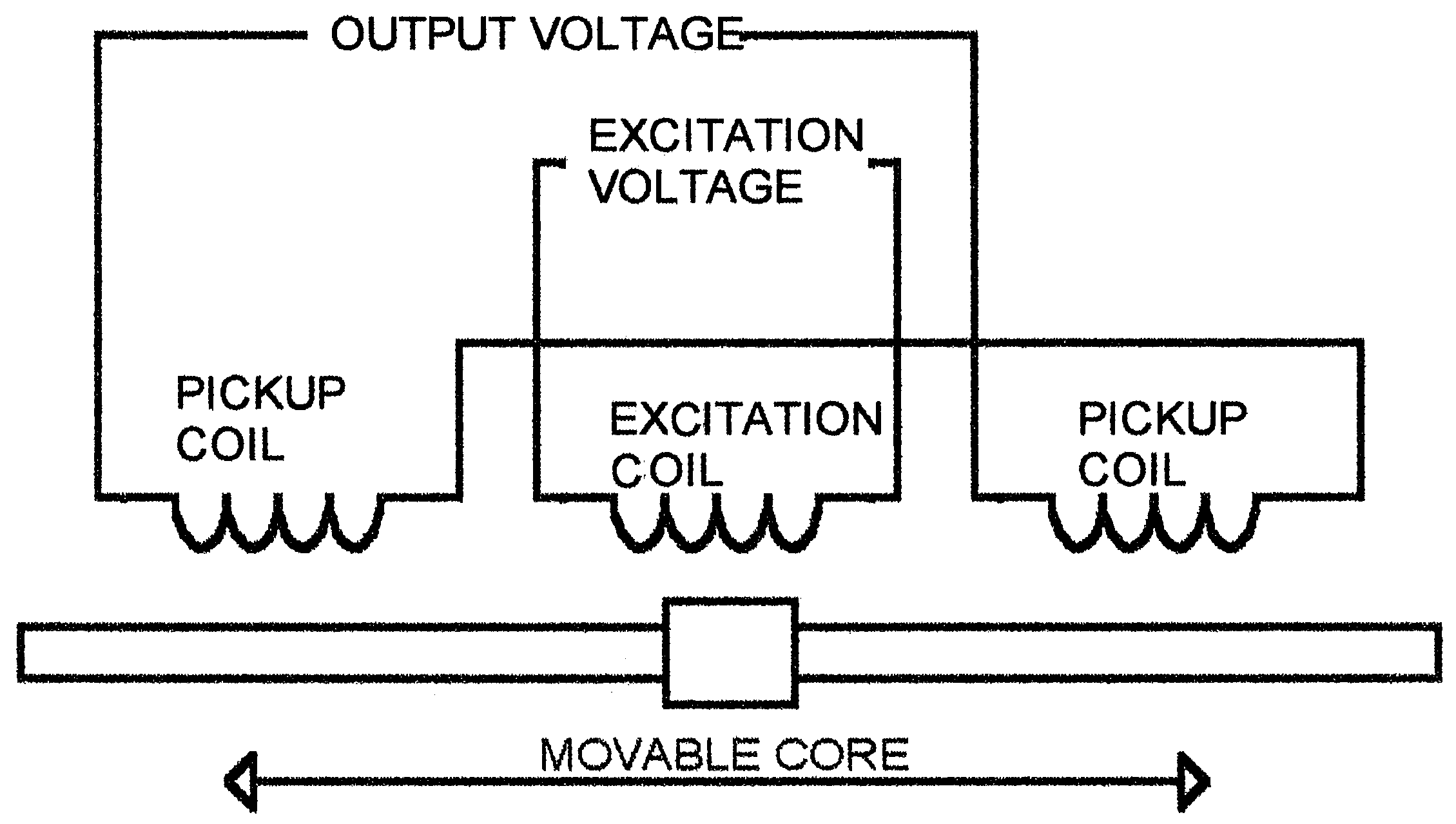
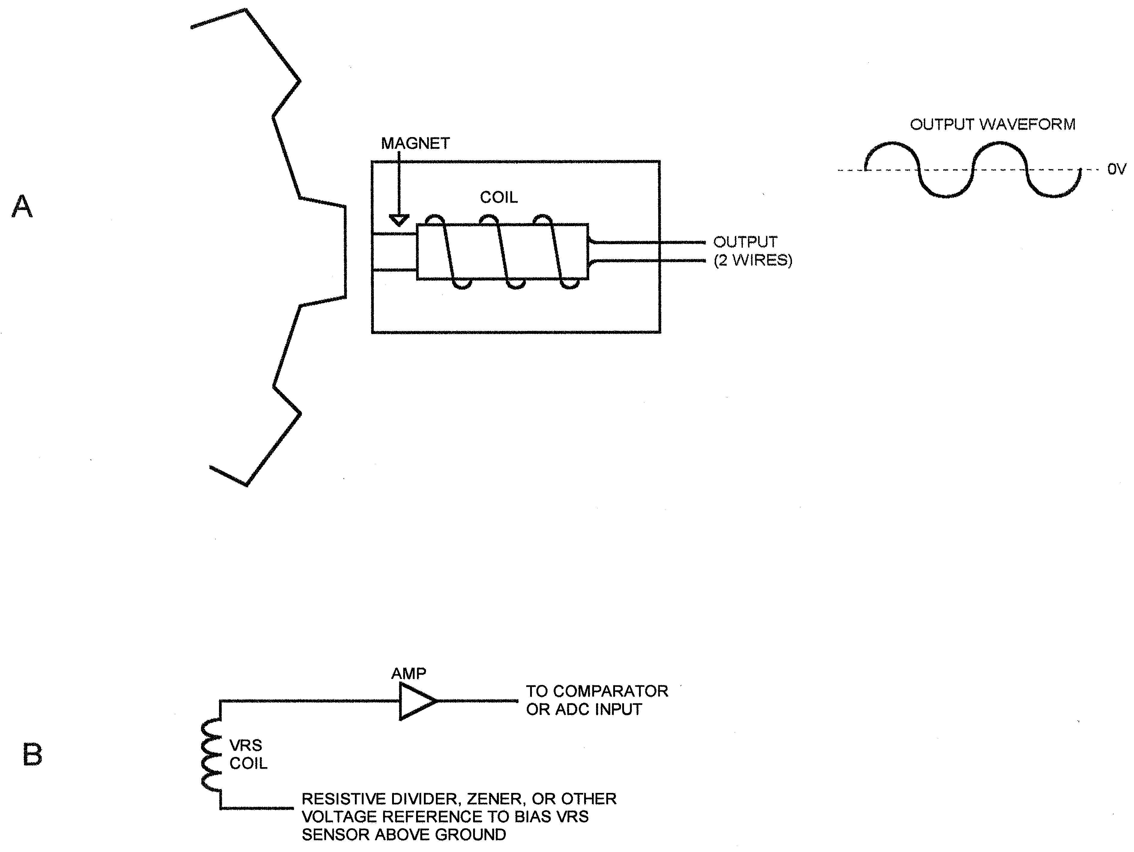


Kõik kommentaarid