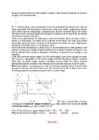
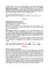
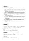
Ticket No11)The
characteristic is called output characteristic or volt-ampere
charateristic of a
Rectifier Diode .
2)Rectifier
Diode .
3)A
is called Anode and C is called Cathode. An Anode has
positive potential and
therefore collects electrons in the
device . Cathode has
negative potential and therefore emits electrons to anode. The
symbol looks like an arrow that ponts from the anode to the cathode, and
reminds that conventional
current flows easily from the p side(anode)
to the n side(cathode).
BIASING.
Forward biasing. If the current in a diode is too large, excessive
heat will
destroy the device. Even approaching the
burnout current
value without reaching it can shorten its life. Therefore manufacturer’s
data sheet specifies the
maximum forward current, that diode can
withstand. This
average current IF is the
rate a diode can
handle up to the forward direction when used as a rectifier.
Another entry of interest in the data sheet is the forward voltade
drop UF(max) when the maximum forward current occurs. An usual
diode has this value 0.7-2.0V. Diode conducts easily when forward
biased .
Reverse biasing. The reverse current is a leakage current at the source
rated
voltage . Typically,
silicon diodes have 1-10 microA and
germanium 200-700 microA of leakage current. This value includes
thermally produced current and surface leakage current. Only
these currents take
place , when a diode is reverse biased. At breakdown,
the diode
goes into avalanche where a number of carriers appear
suddenly in the depletion
layer . With a rectifier diode, breakdown is
usually destructive.
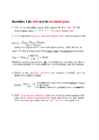
4) Typical values : Uknee- approximatly 0.7V; UF –
0.7-2.0V; leakage (IR) – 1-10 microA/200-700microA.
5)Idealized
characteristic. In view of a very small leakage current in the
reverse-
bias state and a small
voltage drop in the forward-bias state
as compared to the
operating voltages and currents of a
circuit in
which the diode is used, the oputput characteristic of the diode can
be idealized as shown in the
figure . This
corner can be used for
analyzing the circuit topology, but should not be used for actual
circuit design. At
turn on, the diode can be
considered as an
ideal switchbecause it turns on rapidly as compared to transients in the
circuit.
6)
One of its main applications is in rectifiers, circuits that
convert the Alternating voltage or alternating current into
direct voltage or
direct current. It is also applied in detectors, which find the
signals in the noisy
operation conditions . The third application is
in switching circuits because an ideal rectifier
acts like a
perfect conductor when forward biased and lik a perfect insulator when
reverse biased.
7)A
power diode is more complicated in structure and operational
characteristics than the small
signal diode. The forward bias
characteristic of the power diode is
approximately linear , which
means that the voltage drop is
proportional to the omic
resistance and to the current. The rated currents of power diodes are thousands
of amperes and the area of the pn
junction may be tens of
square centimeters.
In
the
case of power diode, the additional n- layer exists
between these two layers, which is termed as a
drift region . This
layer can be quitewide for the diode. The
wide lightly doped region
adds significant ohmic resistance to the forward-biased diode and
causes larger power dissipation in the diode when it is conducting
current.
Most
of the power dissipation in a diode occurs in the forward-biased
on-state operation.
Real poeration currents and voltages of power
diodes are essentially restricted with power
losses and the thermal
effect of power dissipation. Therefore, in power
devices cooling is
very important.
In
the case of reverse biased voltage, only the small leakage current
flows
through the diode. This current is independent of the reverse
voltage
until the breakdown voltage is reached. After that, the diode
voltage remains essentially
constant while the current increases
dramatically.Only the resistance of the
external circuit
limits the
maximum value of current.
8)For
power diodes, switching
process is the most common operation mode. A
power diode
requires a finite time interval to
switch over from the
off-state to the on-state or
vice versa. Switching properties are
analyzed at a given rate of current
change .
The
most essential data of power switching are the
forward voltage
overshoot(UF(max)) when a diode turns on and the
reverse current peak value(IR(max)) when a diode
turns off.
If
Ploss=0, the efficiency is approx. Equial
to 25% 50% 75% 100%
What
are the
sources of current?
carriers electrons neutrons protonsTicket
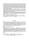
No 2Varactor
Zener diode Bi-directional diode
Schottky LED Photodiode Optocoupler(LED and
photo )
2,
3, 4)Varactor. Zener.
Bi-directional.Sch.Led.
Photodiode.
5)Varactor:
U=1-100V, C=10-100 microF. Zener: Zener=-2.4...-200V. Schottky: on
state voltage drop=0.3V. LED: conducting current=2-
10mA .Voltage
drop=2-3V.
6)Varactor:
+(
higher reverse voltage, smaller capacitance) Bi-direct:+(it
operates in either direction to monitr under-voltage dips and
over-voltage spikes of the ac input) Schottky:+(high
frequency , very
fast ) –(Very low breakdown) LED:+(Low voltage, long life, fast
switching)
7)
Zener:
designed to operate in the reverse breakdown. They are
backbone of voltage
regulators.
Bi-directional:Used for line
filtering . Two Zener
diodes connected
back -to-back. It is used as a filtering device to
protect voltage-
sensitive electronic devices from high-energy voltage
transients.
Schottky: High frequency diode.
Based on the
fact ,
that electrons in
different materials have different absolute
potential energies and the potential energy of electrons in materials
is
lower than the potential energy of the free electrons. Used in
computers, because of the
speed .
LED:Energy is radiated as
light .(in
other diodes as a form of heat). Emits
visible and
invisible light rays when forward current through it exceeds the
turn-on current.Used in lamps.
Photodiodes:A window lets light
pass through the packageto the junction. The
incoming light produces
free electrons and
holes . The stronger the light, the
greater the
number of minority carriers and the larger the reverse current.
Optocoupler: LED on the input side and photodiode on the
output side. Light from the led hits the photodiode and this
sets up
a reverse current in the output circuit.
8)How
many valence electrons a germanium
atom has?
1 2 4 8How
is it called the n-type
semiconductor ?
donor recipient acceptor dipolTicket
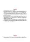
No31,2) Collector characteristic(output characteristics) and input characteristic of
Bipolar Junction
Transistor (BJT)
3)A
junction transistor has three doped
regions . The
bottom is the
emitter,
middle is
base and top is collector.A transistor has two
junctions on opposite
sides of a
thin slaf of semiconductor
crystal :one between the emitter and the base and another between the
bas and the collector. Transistor is
similar to two back-to-back
connected diodes. For normal operation, the emitter diode is forward
biased and the collector diode is reverse biased.(Reverse
biased) (Schematic
symbols of npn&pnp).Three different currents: IE,IB,IC.
5)(Common
emitter, Common base, Common collector.)A:Common emitter input signal
drives the base whereas the output signal occurs between the
collector and the emitter. It is the most popular circuit because of
its high flexibility and
gain .B:Common base input signal drives the
emitter whereas the output signal occurs between the collector and
the base. This
connection is
known as low-gain circuit with high
frequency selectivity Q. C:Common collector input signal drives the
bae, and the output signal
comes from the emitter.
7) Beta :The
ratio of the collector current IC to the base current IB
is called a current gain or a static gain or dc beta of a transistor
and is expressed as β=IC/IB. This
parameter is
also called a forward-current transfer ratio. It is the main property
of the transistor in the CE connection. The current gain of a
transistor is an unpredictable quantity and may
vary as much as a 3:1
range when
changing in the temperature, the
load , and from one
transistor to another.
Alpha :the dc alpha of a transistor
indicates how
close in value the collector current and the emitter
current are.It is defined as:α=IC/IE.Alpha
gain is the main property of the transistor in the CB connection.
Consequently,a
formula of alpha gain in terms of beta is: α=β/(β+1).
Alpha gain is always less than 1 and is
near 1. Both gains depend on
the signal frequency.In the data sheets, the
limit frequency is
shown, which reduces dc beta to 1.
8)Devices
used in power applications are called Power Bipolar Transistors.Small
signal transistors can dissipate
half a
watt or less. Power
transistors dissipate more values.This rating is the limit of the
transistor currents, voltages and other quantities,which are much
higher than those of small-signal devices.In mos applications, power
bipolar transistors are used in a CE circuit with the base as an
input and the collector as output.In power electronic circuits
bipolar NPN are more common than PNP.The base thickness must be made
as small as possible in
order to have a high amplification effect,
but too small base thickness will
reduce the breakdown voltage
capability.The
allowed max voltage UCE between the
collector and the emitter depends
slightly on the base current.
Since the current gain of power bipolar transistors is small, two
transistors are usually connected as a
pair .It’s called Darglington
transistors.The emitter of the
first transistor is connected to the
base of the second one.A connected pair of bipolar transistors
could raise the current gain of a power device.The
difference between power
and low current transistors is, that power transistors have
primary and secondary breakdown area in output characteristics.After primary
breakdown, the transistor can operate, but the secondary breakdown
destroys the transistor completely.As a
result , a narrow
safe operating area is the remarkable disadvantage of the transistor.
If
Pin
= Pout,
the efficiency is approx. equal to:
25% 50% 75% 100%How
many electrons a silicon atom has?
8 14 24 32Ticket
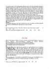
No4
1,2)A:
Junction
Field-Effect Transistor (
JFET ) output characteristic.
B:Input
curve of a
JFET.
C:
Transconductance curve of Metal -Oxide Semiconductor Field-Effect Transistor(
Depletion
mode- MOSFET ).
D:Input curve of
enhancement-mode MOSFET.
3)JFET:MOSFET:Enh-modeMOSFET:
4)JFET:Lower
lead is called source, and the
upper lead is the drain.To produce a
JFET,two
areas of a p-type semiconductor into the n-type
semiconductor have been diffused.Each of these p regions is called a
gate .Most JFETs have the two
gates joined internally to achieve a
single external gate lead, tuhus the device acts, as though it has
only a single gate.In JFET the gate-source diode is always reverse
biased.Because of this, only a very small reverse current can
exist in the gate lead.
Depletion-modeMOSFET:
Figure shows a structure and a way to bias an n-
channel depletion-mode MOSFET with a p-region called a substrate.In its most
basic form, the mosfet looks like a voltage-controlled
resistor , the
resistance of which varies nonlinearly with the input voltage.In the
on-state, tis resistance can be less than 1ohm, while in the
off-state, the resistance increases to
several hundreds of megaohms,
with picoampere leakage currents.
Enhancement-mode
MOSFET:When
the gate voltage is positive enough, electrons fill all the holes
touching the silicon dioxide. The effect is the
same as creating of a
thin layer in n-type material next to silicon dioxide.This conducting
layer is called an n-type inversion layer.The normally of device
suddenly turns on and free electrons
begin to flow easily from the
source to the drain.
5)Unlike
JFET, MOSFETs metallic gate is electrically insulated from the
channel by a thin layer of silicon dioxide.Because of this, the input
resistance is evene higher than that of a JFET.Ability to use a
positive gate voltage distinguishes MOSFET from JFET.Depletion mode
MOSFET has an n-channel between the source and the drain.
Enhancement-mode MOSFET doesn’t have an n channel.And also
enhancement-mode MOSFET is normally off when the gate voltage is
zero , whereas a depletion-mode device is normally on.
6)Advantages
of JFET:a)Due to the voltage adjustment, the
control circuit is
simple with a low control power;b)because a JFET is an
electron majority carrier device, the switching transients speed
grows essentially;c)for some
reason , its on-state resistance has a positive
temperature coefficient, that is the resistance rise with the
temperature rise;d)accordingly, the current
falls with the load and
the
parallel connection of
such devices is not the problem;e)due to
the absence of the second breakdown, the safe operating area is
large, therefore the overvoltage
protection is not
needed.
Disadvantages :a)due to the high transistor resistance
of the current flow, the efficiency of FET is not high when a number
of transistors are connnected in parallele;b)the additional losses
between the source and the drain complicate the control
processes.
Advantages of MOSFETs:a)high speed switching
capability, that is the operational frequencies up to 10GHz with the
transient speed 10-100ns because of
almost no
saturation ;b)switching
of positive and negative voltages and conducting of positive and
negative currents with equal
ease ;c)simple protection
circuits;d)simple voltage control;e)normally off device if the
enhancement-mode MOSFET is used;f)positive temperature coefficient
makes it
easy to be applied for parallel devices for increased
current-
handling capability.
Disadvantages:a)relatively low
power handling capabilities(less than 10kVA,
1000V , and 200A);power
losses are proportional to the square of current value.b)relatively
high(more than 2V) forward voltage drop, which results in higher
losses than BJT.
7)ID(max)=2-50A;UDS=60-500V,UG(max)=+/-
20V
8)Power
enhancement-mode MOSFET.The structure of a semiconductor is
composed of many thousands of cells connected in parallel to achieve
a large gain and low on-state resistance.
Overall , the input curve of
a power MOSFET is
quite linear compared with the
parabolic transfer
curve of a small-signal MOSFET.Threshold voltage is
2-4V.
Double -diffused transistor(DMOS) is a kind of a power
MOSFET.The device is fabricated on a lightly doped n-type substrate
with a heavily doped region at the bottom for drain contact.Two
diffusions are used, one to create the p-type
body region and another
to created n-type source region.Breakdown voltage up to 600V and
current capability up to 50A.
How
many electrons a germanium atom has?
8 14 24 32Holes
are the minority carriers in which type of semiconductor?
n-type p-type each never Ticket
No51)Insulated
Gate Bipolar Transistor (IGBT)
2,3)OutputcharacteristicsInput
characteristics
Typical
graphs of collector current
versus frequency.
4)IC(max)=30-
600A ;UCE=120-1200V
5)Structure
is quite similar to enhanced-mode MOSFET.The principal difference is
the presence of p layer that
forms the collector of the IGBT.This
layer arranges the pn junction which injects minority carriers.
6)7)Advantages:a)the
highest power capabilities up to 1700 kVA,2000V,800A;b)
thanks to the
lower resistance than that of the MOSFET,the heating losses of the
IGBT are low too;c)highest switching capabilities;d)forward voltage
drop is 2-3V, that is higher than that of a bipolar transistor but
lower than that of the MOSFET;e)relatively simple voltage controlled
gate
driver and low gate current;f)the
reliability is higher than
with the FET thanks to the absence of a secondary breakdown.
8)The
leading manufacturer of IGBTs International Rectifier classifies the
production by the
four categories:1)“W“-warp speed devices for 17
to 150kHz;2)“U“-ultra fast speed devices for 10 to
75kHz;3)“F“-fast speed devices for 3 to 10kHz;4)“S“-standard
speed devices for 1 to 3kHz.
If
Ploss
= Pin, the efficiency is approx. equal to:
25% 50% 75% 100%Atomic number is equal to the number of:
carriers electrons neutrons protonsTicket
No61,2)Output
characteristics of Thyristors.
3)A
silicon-controlled rectifier(SCR)
consists of a four-layer silicon
wafer with three pn junctions.It has four doped regions;the anode,the
cathode, and the gate.The gate is the control lead.The SCR is
triggered into conduction by applying a gate-cathode voltage, which
causes a
specific level of gate current.When the SCR is turned off,
it stays in a non-conducting state until it recieves another
trigger.Therefore the SCR can be termed as one-operation thyristor or
rectifier thyristor.
B)the anode-side SCR with an n-gate
lead
.C)the cathode-side thyristor with a p-gate lead.
C)most
common device.
5)Input
characteristic:The
curves show the relation between the gate current and the gate
voltage.This relation has a
broad coherence area with a
width that
depends on the temperature and design properties of the device.The
gate current has an effect upon the form of the characteristic.The
value of a breakover voltage is the
function of the gate current. The
more the gate current, the lower level of voltage is
required to
switch on the thyristor.
6)Figure
reflects the current and voltage transients of a thyristor when it
turns on after a gate pulse
appears and turns off after the current
direction
changes .
During the thyristor opening process, the anode
current will be distributed through the
full crystal surface.The
current distribution is not homogeneous.The turn-on process includes
three time intervals:the turn on delay t0, the current
rise time t1 and the current spreading timet2.The
turn-off process is similar to the diode.For that, the anode current
must be kept well below the
hold current.The decreasing rate of the
current depends on the circuit inductance.The
density of excess
carriers will diminish by the recombination.
7)Diac
is a bi-directional diode that can be triggered into conduction
by reaching a specific voltage value.The diac can pass current in
either direction.This is the current-voltage characteristic.A diac
has neither an anode, nor a cathode.Its
terminals are marked as
MT1(main terminal1) and MT2(main terminal2).
Triac(bi-directional
thyristor) is a three
terminal five-layer device capable of
conducting current in both directions. It is identified as a three
electrode ac semiconductor switch that switches conduction on and off
during each
alternation .its terminals are:MT1;MT2 and G(gate).
8)Triacs
can operate in power
modes of 1,5kV and 100A.
If
Ploss
= Pout,
the efficiency is approx. equal to:
25% 50% 75% 100%If
a transistor has an emitter current of 10mA and a collector current
of 9,95mA, what is the base current (A)?
0,05 19,95 50 19950Ticket
No71)Emitter-follower
.2)The
base ac voltage produces an emitter ac current.Thanks to the limiting
resistor RB and the coupling
capacitor CB, an
ac voltage appears at the emitter.The biasing is arranged with the
help of R1 and R2.Because of the output
capacitor C, this voltage is coupled to the load.Since the emitter is
no longer at ac
ground , the ac voltage across the emitter is
approximately equal to the input voltage at the base.The reason the
circuit is called an emitter follower is because the output voltage
follows the input voltage.
3)4)current,ac,feedback.
5)analog,
class A
6)7)ADVANTAGES:The
output impedance is significantly lower than the inpud impedance.That
is, the circuit is especially useful to decrease the output
resistance of the electronic device.Another benefit is, that almost
no distortion of the signal occurs.That is why the emitter follower
is often used as an
intermediate stage of a power
amplifier for
current amplification.DISADVANTAGES:high noise and limited frequency
range, over which the stabilization is effective.Phase delay.DC
stops.Additional area, volume,
size , weight of amplifiers.
8)If
Vrms
= 10, then Vpeak-to-peak
sin is
approx. equal to:
10 30 60 90What
is the current gain with an input current of 5A
and an output current of 10mA?
2 50 2000 5000Ticket
No81) Differential amplifier, or
diff amp circuit.
2)3)Figure
presents a general form of a diff amp that is termed a long-tailed
pair because RE is called a
tail resistor.It has two
inputs:U1 and U2.Because
there are no coupling or bypass capacitors, the input signals can have frequencies all the way down to zero,
equivalent to dc, and the amplifier has a broad midband and high
stability.The output signal is the voltage on the load connected
between the collectors.Ideally, the circuit is symmetrical with
identical transistors and collector resistors.
4)dc,voltage
device.
5)analog.
6)ADVANTAGES:Because
there are no coupling or bypass capacitors, the input signals can
have a wide range of frequencies and the amplifier has a broad
midband and high stability.Other benefits are high amplification and
low clipping.MAIN
FEATURES :Signal range,offset and drift,kind of
supply .
7)To
obtain higher voltage gain of an amplifier,one can connect two
stages.This is called cascading of the stages and means the amplified
voltage out of the first transistor is coupled into the base of the
second transistor.The second transistor then amplifies the signal, so
that the signal is much higher than the input signal.
Ticket
No91)Schematic
diagram of the operational amplifier(op amp).
2)The input stage
is a diff amp using pnp transistors T1 and T2. T6 forms an
active load that replaces the tail resistor.R2 and D2 control the bias on T6
which produces the tail current of the diff amp.Instead of using an
ordinary resistor,the active load T3 is used.Because of this, the
voltage gain of the diff amp is high.The amplified signal from the
diff amp drives the base of T4,which is and emitter follower.This
stage avoids the loading down of the diff amp.The signal out of T4
goes to T5.Diodes D4 and D5 are
part of the biasing for the
final stage.T7 is an active load for T5.Therefore, T5 and T7 are like a CE
stage with a very high voltage gain.The amplified signal of the CE
stage goes to the final stage,which is a class B emitter follower T8
and T9.Thanks to the balanced supply,the output is 0V when the input
voltage is zero.
3)The
input signal determines the output voltage
swing requirement of the
op amp.There are a number of single-supply amplifiers with inputs
that range from 0V to the positive supply voltage.However,the input
range can be set so that the signal only goes to
within a few
hundred millivolts of each rail.In many single-supply applications it is
required that the input common-mode voltage range extends to one of
the supply rails.
4)dc,
voltage,feedback.
5)analog
7)FEATURES:high
gain, high input resistance,low output resistance,controlled
bandwidth
extended to dc.ADVANTAGES:high frequencies,direct coupling.
8)How
many electrons are there in the valence orbit of a silicon atom
within a crystal?
8 14 24 32What
is the current gain of a bipolar transistor?
IC/IB IE/IB IC/IE IE/ICTicket
No101) Left one:Frequency response of
passive low-pass
filters ;Second:Frequency
response of passive high-pass filters;Third:Frequency response of
passive
band -pass filters;Right:Frequency response of passive
band-stop filters.
2)Filters.
3)Circuit
diagram for Low-pass filters:RC&LC:Passive
high-pass filters:
Passive
band-pass
filter :Passive
band-stop filter:
4)5)Low-pass
filter reduces high-frequency particles
of a signal and passes its low frequency part.
High-pass
filter is
open for high frequencies and
attenuates the low-frequency signals.
Band-pass
filter:at very low frequencies, the
series capacitor looks open to the input signal and there is no
output signal.At very high frequencies,the shunt capacitor looks
short circuited,and there is no ouput also.In between these
extremes,the output voltage reaces maximum value at the
resonant frequency.
Band-stop filter:circuit
with almost zero output at the
particular frequency and
passing the
signals, the frequencies of which are lower or higher than the cutoff
frequencies.
6)7)low-pass&high-pass:
fc=1/(2πRC);fc=1/(2πSQRT(LC))
band-pass:fr=1/(2πSQRT(L1C1))
or fr=1(2πSQRT(L2C2)):f2-f1=R/(πL1)=1/(πC2R).
band-stop: f2-f1=R/(4πL2)=1/(πC1R)
8)If
Vpeak-to-peak
sin =
100, then Vrms
is approx. equal to:
10 30 60 90When
is the atom said to be in
electrical balance?
electrons=protons electrons=holes electrons=carriers carriers=holesTicket
No111,2)Left:op
amp suming amplifier(
summer or
adder);Second:Integrator;Third:Differentiator;Right:Proportional-
integrated -differential
circuit(PID).
3)4)input
and output signals are on the circuits.
5)summer:the output is
the sum of the input voltages.Integrator:produces a
ramp of output
voltage,which is a linearly increasing or decreasing
voltage.Differentiator:produces an output voltage proportional to the
instantaneous rate of change of the input voltage.PID:They amplify
the
beginning and the end of the pulse
signal.
6)Summer:Uout=-(U1R/R1+U2R/R2+U3R/R3).
Integrator:Uout=-1/T
int(Uindt);Iin=Uin/R;Uout=-Iint/C
= -Uint/T;Uout= -Uin/(4fT).
Differentiator:Uout=
-T dUin/dt.
PID:K=R2/R1;T1=
R1C1 ;T2=R2C2
7)Substracter:The
output voltage,which is proportional to the difference of the input
voltages when R1=R2 and R=R3.
Logarithmic:It
is the inverting amplifier with a feedback diode rather than feedback
resistor.
Once the diode and the resistor positions
replace on other,
the
exponential amplifier appears:
In
case of the positive feedback, the midband becomes
: larger narrow no matter no bandWhat
is the main
action of electrons in the base of an npn transistor?
recombination flowing -out doping ionizationTicket
No121,2)Switches(switching
circuits).Left:
Inverter ;Second:
Multiplexer;Third:
Comparator;Right:
Latch .
3)Switching
devices.
4)Switching transistor circuits are known as class B
operation devices.It means, that the collector current flows only one
half of ac.For this to occur, the Q point is located at cutoff on
both the dc and ac load lines. Transistors are, because
transistorized base bias is usually designed to operate in switching
circuits by having either low output voltage or high output
voltage.
5)on circuits.
6)Inverters output voltage is in
the opposite polarity to the input voltage.
Multiplexer is a
multiple switch that steers one of the input signals to the
output.
Comparator:perfect solution for comparing one voltage
with another to see which is larger.
Latch:because the
collector of T1 drives the base of T2 and vice versa,it is a positive
feedback.Achange in current at any point of the
loop is amplified and
returned to the starting point with the same phase.
7)Advantages
of swithces:Extremely low power consumption and lower heat
production.Physically small.They can
provide large load currents at
low voltages although they produce more electrical and audible
noise.
Adv of comparator:fast differential dc amplifier of high
gain and stability.
Disadv:need high resolution which implies
high gain.
8)Sample-and-hold
circuit(SHA)It
captures an analog signal and holds it during some operation.When the
SHA is in the hold mode, the output is closed.When the SHA is in the
sample mode, the output follows the input with a small offset equal
to the hold period.The energy storage device, the
heart of the SHA is
acapacitor.
RS flip - flop :Each
collector drives the opposite base through a resistors RB.One
transistor is saturated and the other is cutoff.Depending on which
transistor is saturated,the Q output is either low or high.RS
flip-flo circuit can set the Q point to high or
reset it to low.High
input S sets Q to high and high input R resets Q to low.
What
does the electron interact with?
hole neutron dipole crystalWhat
does the flowing of electrons in an npn transistor start from?
emitter collector base gateTicket
No131)Oscillators.
2)Left:
Push - pull amplifier;Second:
RS flip-flop;Third:
Blocking
oscillator;Right:
Astable multivibrator.3)Switching.
4)Left one: Class B transistors. Pair of identical
Transistors are there to reduce disortion.So that the signal can be
introduced across.
Right one:The input of the first transistor
amplifier is the output of the second one.Once the current of one
transistor becomes higher the other,the voltage drop of its
collector’s resistor grows.This change is transferred through the
corresponding capacitor to the base of the other transistor so that
the current grows increasingly up to the first transistor saturation
and the second transistor
closing .
Third one:Originally, the
forward biased transistor emits the base of the transistor.The
capacitor charges and
sends the pulse to the transformer.After the
transistor saturation,the feedback signal falls the capacitor
discharges,and the oscillation starts
again .
5)On
circuits.
6)Push-pull:designer arranges the biasing of
push-pull amplifier to set the Q point at cutoff;
RS
flip-flop:designed, that circuit can set the Q point to high or
reset it to low;
Blocking ocillator:Unlike a multivibrator,the
output of this circuit is sharp pulses with
brad pauses between
them.It has also a transformer;
Multivibrator:is a rectangle
pulse generator with the positive feedback.
7)Advantages:simple
principle of operation, low
price , high
reliability.
Disadvantages:unstable and temperature
dependent.Output waveform has distortions and changes with time.
8)Monostables:It
generates the only pulse after switching on, and on
continue operation, an input signal must enter the circuit.The pulse width of
the single-short output signal is
determined by R and C values.At the
initial state, the transistor T2 passes the current and T1
is closed.The capacitor is charged.After Uin enters T1,the
T1switches on and the capacitor closes T2.The
capacitor discharges through R and not T1 but T2
continues conducting thanks to the base current from R1.After
the full discharging of the capacitor,T2 switches on again
and T1 switches off.
In
case of the negative feedback, the midband becomes:
larger narrow no matter no bandHow
many valence electrons a silicon atom has?
1 2 4 8Ticket
No14U1U2NOT U1U1 OR U2U1 NOR U2U1 AND U2U1 NAND U20010101011100110010011101010Mark
the inputs and outputs, each element, and all signals of the
circuits.
Fill in the truth table.
Draw the circuit diagrams of the devices that implement the columns of the table.
What each device is called?
Draw the schematic symbol of each device.
Draw the input and output signals of these five devices.
Are there analog, switching, or digital devices? They are build on the digital gates- dig. Devices. You can make switching devices of them
Inscribe the logical equation that each circuit solves. OR+,AND*,NOT-,
Draw other circuits of such kind and describe their elements and performance .
Round the true answers
How many electrons are there in the valence orbit of a germanium atom within a crystal? 8
The base of a bipolar transistor is made of: semiconductor
Ticket
No15
diode
thyristor
The Main Problem
Mark
the inputs, outputs, and each element of the circuit.
What device this circuit diagram belongs to? Forward biased diode circuit
Plot the voltage and current waveforms of this device.
Inscribe the axes and mark the specific regions and points of the characteristics.
What are the typical values of the quantities in the points, which you have marked?
Tell about the powers, voltages, and currents of the device. It is a nonlinear device meaning that its output current is not proportional to the voltage. Easy direction of electron flow is against the diode arrow. Its typical bulk resistance is less than 1 oom and forward voltage drop between 0.7 and 2 V. Due to high reverese resistance, a diode has a low leakage current. At breakdown, the diode goes into avalvance that may destroy it. The current is small for the first few tenths of a volt. Above knee voltage, the slightest increase in diode voltage produces a large growth in current. If the current is too large, approaching to the burnout current, the excessive heat will destroy the device. Closely related to the max forward current and forward voltage drop is the maximum power dissipation that indicates how much power the diode can safely dissipate without shortening its life.
Plot the same waveforms for the circuit built on the thyristor instead of the diode.
List the advantages and disadvantages of these devices.
- Easy to destroy the device by too high voltage, current or frequency values
- Large currents cause significant voltage drops
- It can convert alternating current/voltage into direct one
- Can be applied in detectors, which fin signal in noisy condtitions
- Used as a switch also, ideal rectifier acts like a switch that closes the current flow when foward biased and opens it when reverese biased
Round the true
answers
What is resistance of metal due to? voltage current ionization vibration
What are the majority carriers in the base of an npn transistor?
electrons holes protons neurons


Kõik kommentaarid