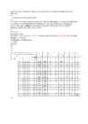
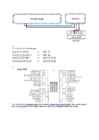
Mictrocontroller Week 03 Numbering systems 1. Convert the decimal number 123.456 to the following formats, taking whole numbers and fractions into account. Show calculations. a) Binary Fractional part : Reading direction Integral part: Reading direction 0,456 x 2 = 0,912 0 123 / 2 = 61 1 0,912 x 2 = 1,812 1 61 / 2 = 30 1 0,812 x2 = 1,624 1 30 / 2 = 15 0
Cat. No. W317-E1-11 SYSMAC CPM1A Programmable Controllers OPERATION MANUAL CPM1A Programmable Controllers Operation Manual Revised October 2007 iv Notice: OMRON products are manufactured for use according to proper procedures by a qualified operator and only for the purposes described in this manual. The following conventions are used to indicate and classify precautions in this manual. Always heed the information provided with them. Failure to heed precautions can result in injury to people or dam- age to property. ! DANGER Indicates an imminently hazardous situation which, if not avoided, will result in death or serious injury. Additionally, there may be severe property damage. ! WARNING Indicates a potentially hazardous situation which, if not avoided, could result in death or serious inju
Analog Interfacing to Embedded Microprocessors Real World Design Analog Interfacing to Embedded Microprocessors Real World Design Stuart Ball Boston Oxford Auckland Johannesburg Melbourne New Delhi Newnes is an imprint of Butterworth–Heinemann. Copyright © 2001 by Butterworth–Heinemann A member of the Reed Elsevier group All rights reserved. No part of this publication may be reproduced, stored in a retrieval system, or transmitted in any form or by any means, electronic, mechanical, photocopying, recording, or otherwise, without the prior written permission of the publisher. Recognizing the importance of preserving what has been written, Butterworth–Heinemann prints its books on acid-free paper whenever possible. Library of Congress Cataloging-in-Publication Data Ball, Stuart R., 1956– Analog interfacing to embedded microprocessors : real world design / Stuart Ball. p. cm. ISBN 0-7506-7339-7 (pbk. : alk. paper) 1. Embedded computer
oData transparency: In bit and byte oriented protocols, there is a problem if a control character (for ETX (End of Text) ·Same as ETB, only no more blocks will follow. ITB (End of > Differences with HDLC length of protocol field (1B or 2B) byte-oriented protocols) or the start-of-frame flag (for bit-oriented protocols) appears in the actual data. Intermediate Transmission Block) ·Same as ETB, except that the receiving statio Differs from HDLC because of multiaccess MAC that provides · Maximum payload length (default: 1500) This was not likely to happen in ASCII text, but is very likely with binary data. This is known as a data will not acknowledge after the error checking. EOT (End of Transmission) framing/error detection: · Type of CRC (2B or 4B) transparency problem an can be rectified with byte stuffing (for byte-orien
tutvu lausearvutuse keskkonnaga: http://logik.phl.univie.ac.at/~chris/gateway/formular-uk-zentral.html Millistel muutuja väärtustel on lause (Av(B&A))v(-A&(Cv(B&-C))) väär? Panna tuleb results only, 0 on väär 1 on õige Tutvu ajalooga saidis kuni II maailmasõda: http://www.maxmon.com/history.htm Loe läbi jutt ja proovi andmetega mängida: http://math.hws.edu/TMCM/java/DataReps/index.html Kahend süsteemi arvu(101101001) ->kümnend süsteemiks. Nr sisse ja bianarile punkt, ja vaatan base ten integeri kümnendarvudest annab Ecki appletis juuresoleva graafilise kujutise, teen kujundi ja vaatan base integeri mis vastab kahendsüsteemi arvule 1110001 ASCII tabelis? Nr sisse ja punkt bianari, vaatan ...teksti Kümnendsüsteemi arv 33 on kahendsüsteemis? 33 kirjutan ja Base-ten integer, vaatan bianary Loe läbi jutud Atbashi ja Caesari šifri (Caesar cipher) kohta: http://www.wikipedia.org 2 Tutvu ajalooga kuni 1970ndad: http://www.islandnet.com/~kpolsson/comphist/ 47-68 ingli
Homework 1. a)123/2= 61,5; 61/2=30,5; 30/2=15; 15/2=7,5; 7/2= 3,5; 3/2=1,5 (1111011) 0.456*2=0.912; 0,912*2=1,824; 0,824*2=1,648; 0,648*2=1,296; 0,296*2=0,592; 0,592*2=1,184; 0,184*2=0,368; 0,368*2=0,736; (0,736*2=1,472; 0,472*2=0,944; 0,944*2=1,888) So b)123/16= 7,6875 ; 0,6875*16=11 ; 7/16 is less than one, then hex is 7B 0,456*16= 7,296 ; 0,296*16=4,736; 0,736*16=11,776; 0,776*16=12,416; 0,416*16=6,656; 0,656*16=10,496; 0,496*16=7,936; 0,936*16=14,976; 0,976*16=15,616; 0,616*16=9,856; 0,856*16=13,696; 0,696*16=11,136; 0,136*16=2,176; 2,176*16=2,816; 0,816*16=13,056 Hex is 7B.74BC6A7EF9DB22D c) 123,456/5=24,6912/5=4,93824/5=0,987648 0,987648*5=4,93824; 0,93824*5=4,6912; 0,6912*5=3,456; 0,456*5=2,28; 0,28*5=1,4; 0,4*5=2; 0*5=0 base-5 is d)BCD is 2. a) Unsigned 16-bit binary is 0000000001101011. Hexadecimal is 6B b) Unsigned 16-bit binary is 0000000010110101. Hexadecimal is B5 3. a) Signed two's c
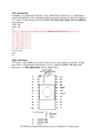
Motherboard - the principle printed circuit board assembly in a computer; includes core logic (chipset), interface sockets and/or slots, and input/output (I/O) ports. Printed circuit board (PCB) - a thin, laminated sheet composed of a series of epoxy resin and copper layers and etched electronic circuits (signal, ground and power) Chipset (or core logic) - two or more integrated circuits which control the interfaces between the system processor, RAM, I/O devises, and adapter cards. Processor slot/socket - the slot or socket used to mount the system processor on the motherboard AGP - Accelerated Graphics Port - a high speed interface for video cards; runs at 1X (66MHz), 2X (133MHz), or 4X (266MHz). PCI - Peripheral Component Interconnect - a high speed interface for video cards, sound cards, network interface cards, and modems; runs at 33MHz. ISA - Industry Standard Architecture - a relatively low speed interface primarily used for sound cards and modems; runs at approx. 8MHz. RAM - Ran
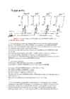
Question 1 Define the following ADC terms: 1. SNR – (Signal to Noise Ratio) SNR is a calculated value that represents the ratio of RMS signal to RMS noise. 2. SINAD - (signal-to-noise-and-distortion ratio) Ratio of the RMS signal amplitude to the mean value of the root-sum-square (RSS) 3. ENOB – (effective number of bits) The effective number-of-bits and relates to SINAD 4. THD - (total harmonic distortion) Ratio of the rms value of the fundamental signal to the mean value of the RSS of its harmonics. 5. SFDR - (spurious free dynamic range) Ratio of the RMS value of the signal to the RMS value of the worst spurious signal. 6. Channels - related to the inputs of the ADC can either be multiplexed or individually selected. 7. Linearity - relates to how a ADC follows a linear function. All ADCs are to a certain extend nonlinearity. 8. Operating temperature - measurement, which i


Kõik kommentaarid