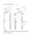
Tallinn University of Technology Department of Electrical Drives and Power Electronics Report on Exercises 2 Diodes Student ******* Code ****96 Group AAVB41 Tallinn 2012 2.1. Diode rectifier VD f = 9 kHz U=6V U = 19.7 V R = 96 k Figure 1. Circuit diagram Figure 2. Timing diagram
Diodes Tallinn 2011 + A VS RV V D - Fig. 1.1. Circuit diagram VS - DC voltage source PS 5005, 0-50VDC/0-5A RV - Rheostat, Rmax=3600 V - DC volt meter DV-101, 200mV-200V A - DC current meter DA-103, 2mA-20mA-200mA-5A D - Diode 1N360 Voltage divider calculations RV=(US-UAC)/If(max) RV=(46,6 - 0,45)/0,1=461,5 Table 1.1. Observed data If , mA US If Uf Ir Ur 0,60 - 1,1 3 0 4,9 0,67 - 5,1 2 0 10 0,70
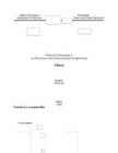
Department of Electrical Drives and Power Electronics Report on Exercises 2 on Electronics and Semiconductor Engineering Filters Student AAVB-41 Tallinn 2008 Exercise 2.1. Low-pass filter Circuit diagram Timing diagram and frequency responses High-pass filter Circuit diagram Timing diagram and frequency responses Calculations Quantity Calculated Experimental value value Umax, V 14,14 14,14 I, mA 0,0044 0,0044 UR, V 4,47 4,4 UC, V 8,944 8,978
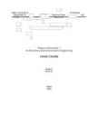
Tallinn University of Technology Department of Electrical Drives and Power Electronics Report on Exercises 1 on Electronics and Semiconductor Engineering Linear Circuits Student AAVB-41 Tallinn 2008 Exercise 1.1. RL circuit Quantity Calculated Experimental value value Umax, V 14,14 14,14 I, mA 983 983 UR, V 9,82 9,81 UL, V 1,85 1,85 -10,7 -10,6 -2,0 -1,7
Ticket No1 1)The characteristic is called output characteristic or volt-ampere charateristic of a Rectifier Diode. 2)Rectifier Diode. 3) A is called Anode and C is called Cathode. An Anode has positive potential and therefore collects electrons in the device. Cathode has negative potential and therefore emits electrons to anode. The symbol looks like an arrow that ponts from the anode to the cathode, and reminds that conventional current flows easily from the p side(anode) to the n side(cathode). BIASING. Forward biasing. If the current in a diode is too large, excessive heat will destroy the device.
Department of Electrical Drives and Power Electronics Report on Electronics and Semiconductor Engineering OP AMPS Student AAAB-41 Tallinn 2011 Exercise 5.1. Non.Inverting Voltage Amplifier Fig . Circuit diagram Fig . Diagrams of bandwidth versus gain. Data table Measur Calculated ed Uin R1, k R2, k KU Uout, V fc, kHz KU Uout, V fc, kHz 0,7 2 18,57 9,63 6,74 146 10,29 7,2 150
Tallinn University of Technology Department of Electrical Engineering ELECTRONICS AND SEMICONDUCTOR ENGINEERING Exercises Linear circuits Student: xxxxxxxx Code: xxxxxx Group: xxxxxx TALLINN xxxx 1.1 RL-Circuit L1 100mH Uout=4V V1 232.5 Vrms
Instructor: Prof. Valery Vodovozov Tallinn 1. RC filter R Vnoise 1000Ω 15 Vrms 11kHz 0Deg RL V C1 11kΩ 7.23µF 11.23 Vrms IC=0V 11 Hz 0Deg Figure 1. Circuit diagram of the low-pass RC filter Calculations f = 11 Hz Rc = 11 kΩ UL = 10 V R1 = 1 kΩ fc = 2f = 22 Hz 1 ω=2 πf =2∙ 3,14 ∙ 11 Hz=69,12 s 1 ωC =2 π f C =2 ω=138,24 s 1 1 C= = =7,23 μF ωC R 1 1 138,24 ∙1000 Ω s


Kõik kommentaarid