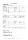
10 00 0000 0000 - 10 11 1111 1111 (0x800-0xBFF) 11 00 0000 0000 - 11 11 1111 1111 (0xC00-0xFFF) Three inputs NAND chip and scheme Scheme used four of the PROM chips and four three-input NAND gates (CS = chip select pins) Scheme to coonect 12 input pins MP address to four PROM 10 address pins == MEMR (Merory Read) 11. You are designing a multi-user interface that stores user preference data on external memory. You decided to use a PIC18F45K20 microcontroller and 24C02C EEPROM memory. Your microcontroller needs to generate a block wave that will act as a clock signal to synchronize data transfer to and from the memory. a) Choose a suitable clock frequency, based on the capabilities of the EEPROM module and the PIC. b) Assume the clock frequency of the PIC is 16 MHz and one instruction cycle lasts 4 clock periods. Further assume that one loop of your algorithm requires 4 instruction cycles
CS CS CS A9 A9 A9 0 A10 1 DC 2 A11 3 11. You are designing a multi-user interface that stores user preference data on external memory. You decided to use a PIC18F45K20 microcontroller and 24C02C EEPROM memory. Your microcontroller needs to generate a block wave that will act as a clock signal to synchronize data transfer to and from the memory. a) Choose a suitable clock frequency, based on the capabilities of the EEPROM module and the PIC. Suitable clock frequency is 0-400 kHz (from datasheet) b) Assume the clock frequency of the PIC is 16 MHz and one instruction cycle lasts 4 clock periods. Further assume that one loop of your algorithm requires 4
-85dB b) MAX1201 pipeline ADC. -85dB c) MAX1205 pipeline ADC. -84dB Question 9 Name two disadvantages of: a) Flash ADC - expensive, high power consumption b) SAR ADC - speed is limited, needs anti-aliasing filter c) Dual-slope ADC -slow conversion, expensive external components required (high accuary components) a) Sigma Delta ADC -multibit ADC and multibit feedback DAC – higher order Question 10 Find the following for the built-in ADC in the PIC18F45K20: a) Architecture - SAR(Succesive Approximation Register) b) Differential linearity - +- 0.4 LSB c) Minimum acquisition time – 1.4ms d) Minimum conversion time – 8.4 𝜇𝑠 Question 11 A 10 bit DAC has a reference voltage of 5.12V. What is the output voltage for a binary input code of 11000100012? 11000100012 = 785 210 = 1024 (5.12/ 1024) * 785 = 3.925V Output voltage = 3.925V Question 12 A 12 bit DAC has a reference voltage of 10V. What is the output