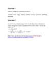
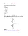
V. Design RF, RH and RL for optimal temperature resolution. Use the range 0.5 – 4.5 V as in Ball Chapter 3. Since we have 8 bit = 256 step resolutions -10°C corresponds 3.35/5 *256 = 171 to 50°C corresponds 1.02/5 * 256 = 52 to 8 bit ADC steps of 171-52=119 counts for 50C to -10C = 60C span Therefore, the resolution is 119 =1,98 steps 60 We want the -10°C to 50°C falling between 0.5V to 4.5V on the ADC: This caling will give 8bit ADC range of 204 counts over 60C span. 204 =3,4 steps 60 Before scaling, the output V0 span is 3.35V- 1.02V=2.33V. After scaling, the output V0 span will be 4.5V-0.5V=4.0V. 4 / 2.33 =1.7 The gain (amplification) for this will be The outputs will be : 3.35V* 1.7 = 5,7V and 1,02v * 1.7 = 1,73 The offset will be 1.73V -0.5V = 1.23V V R ∙ RF =1.23 RH VR= 5 V and RF= 10kΩ
119counts Therefore, the resolution is 1.98 steps 60span We have: RF RF V R VOUT VSensor (1 ) R F RL RH RH R R V R where (1 F F ) is the gain and R F is the offset. RL RH RH We want the -10°C to 50°C falling between 0.5V to 4.5V on the ADC: This caling will give 8bit ADC range of 204 counts over 600C span. 204counts Therefore, the new resolution is 3.4 steps 60span Before scaling, the output V0 span is 3.35V-1.02V=2.33V After scaling, the output V0 span will be 4.5V-0.5V=4.0V 4.0V The gain (amplification) for this will be 1.7 2.33V
 annaabi.ee