Piletid vastustega
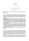
B:Input curve of a
JFET.C:Transconductance curve of Metal-Oxide Semiconductor Field-Effect
Transistor(Depletion mode-MOSFET).D:Input curve of enhancement-mode MOSFET.
3)JFET:MOSFET:Enh-modeMOSFET:
4)JFET:Lower lead is called source, and the upper lead is the drain.To produce a JFET,two
areas of a p-type semiconductor into the n-type semiconductor have been diffused.Each of
these p regions is called a gate.Most JFETs have the two gates joined internally to achieve a
single external gate lead, tuhus the device acts, as though it has only a single gate.In JFET the
gate-source diode is always reverse biased.Because of this, only a very small reverse current
can exist in the gate lead.
Depletion-modeMOSFET: Figure shows a structure and a way to bias an n-channel
depletion-mode MOSFET with a p-region called a substrate.In its most basic form, the mosfet
looks like a voltage-controlled resistor, the resistance of which varies nonlinearly with the
input voltage