Piletid vastustega
Because of this, only a very small reverse current
can exist in the gate lead.
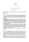
Depletion-modeMOSFET: Figure shows a structure and a way to bias an n-channel
depletion-mode MOSFET with a p-region called a substrate.In its most basic form, the mosfet
looks like a voltage-controlled resistor, the resistance of which varies nonlinearly with the
input voltage.In the on-state, tis resistance can be less than 1ohm, while in the off-state, the
resistance increases to several hundreds of megaohms, with picoampere leakage currents.
Enhancement-mode MOSFET:When the gate voltage is positive enough, electrons fill all
the holes touching the silicon dioxide. The effect is the same as creating of a thin layer in n-
type material next to silicon dioxide.This conducting layer is called an n-type inversion
layer.The normally of device suddenly turns on and free electrons begin to flow easily from
the source to the drain.
5)Unlike JFET, MOSFETs metallic gate is electrically insulated from the channel by a thin