Piletid vastustega
single external gate lead, tuhus the device acts, as though it has only a single gate.In JFET the
gate-source diode is always reverse biased.Because of this, only a very small reverse current
can exist in the gate lead.
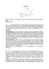
Depletion-modeMOSFET: Figure shows a structure and a way to bias an n-channel
depletion-mode MOSFET with a p-region called a substrate.In its most basic form, the mosfet
looks like a voltage-controlled resistor, the resistance of which varies nonlinearly with the
input voltage.In the on-state, tis resistance can be less than 1ohm, while in the off-state, the
resistance increases to several hundreds of megaohms, with picoampere leakage currents.
Enhancement-mode MOSFET:When the gate voltage is positive enough, electrons fill all
the holes touching the silicon dioxide. The effect is the same as creating of a thin layer in n-
type material next to silicon dioxide.This conducting layer is called an n-type inversion
layer