Tallinn
University of Technology
Department
of Electrical Drives and Power Electronics
Report on Exercises 1
on
Electronics and Semiconductor Engineering
Linear Circuits
Student
AAVB-41
Tallinn
2008
Exercise 1.1. RL circuit
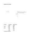
Department of Electrical Drives and Power Electronics Report on Exercises 2 on Electronics and Semiconductor Engineering Filters Student AAVB-41 Tallinn 2008 Exercise 2.1. Low-pass filter Circuit diagram Timing diagram and frequency responses High-pass filter Circuit diagram Timing diagram and frequency responses Calculations Quantity Calculated Experimental value value Umax, V 14,14 14,14 I, mA 0,0044 0,0044 UR, V 4,47 4,4 UC, V 8,944 8,978
Tallinn University of Technology Department of Electrical Engineering ELECTRONICS AND SEMICONDUCTOR ENGINEERING Exercises Linear circuits Student: xxxxxxxx Code: xxxxxx Group: xxxxxx TALLINN xxxx 1.1 RL-Circuit L1 100mH Uout=4V V1 232.5 Vrms
Tallinn University of Technology Department of Electrical Drives and Power Electronics Report on Exercises 3 on Electronics and Semiconductor Engineering Diode circuits Student AAVB-41 Tallinn 2008 Exercise 3.1. Diode characteristics Fig. 3.1. Circuit diagram Timing diagram Output characteristic (forward bias only) Forward Bias Reverse Bias Umax, V UAC, Vrms Measured Calculated IA, Arms IA, Arms 0,5 0,35 0,006 0 1 0,64 0,1 0
Tallinn University of Technology Department of Electrical Drives and Power Electronics Report on Exercises 5 On Electronics and Semiconductor Engineering Op amps AAVB-41 Tallinn 2008 Exercise 5.1. Non-Inverting Voltage Amplifier Fig. 5.2. Diagrams of bandwidth versus gain Data table R1,k Measur ed Calculated Uin,V R2,k K Uout,V fc,kHz K Uout,V fc,kHz 1 90 50 2,80 1,98 530,31 2,8 1,96 535,71 1 90 40 3,25 2,30 457,55 3,25 2,28 461,54 1 90 30 4,00 2,83 372,40 4 2,80 375,00 1 90 20 5,50
Instructor: Prof. Valery Vodovozov Tallinn 1. RC filter R Vnoise 1000Ω 15 Vrms 11kHz 0Deg RL V C1 11kΩ 7.23µF 11.23 Vrms IC=0V 11 Hz 0Deg Figure 1. Circuit diagram of the low-pass RC filter Calculations f = 11 Hz Rc = 11 kΩ UL = 10 V R1 = 1 kΩ fc = 2f = 22 Hz 1 ω=2 πf =2∙ 3,14 ∙ 11 Hz=69,12 s 1 ωC =2 π f C =2 ω=138,24 s 1 1 C= = =7,23 μF ωC R 1 1 138,24 ∙1000 Ω s
Department of Electrical Drives and Power Electronics Report on Electronics and Semiconductor Engineering OP AMPS Student AAAB-41 Tallinn 2011 Exercise 5.1. Non.Inverting Voltage Amplifier Fig . Circuit diagram Fig . Diagrams of bandwidth versus gain. Data table Measur Calculated ed Uin R1, k R2, k KU Uout, V fc, kHz KU Uout, V fc, kHz 0,7 2 18,57 9,63 6,74 146 10,29 7,2 150
Student ******* Code ****96 Group AAVB41 Tallinn 2012 2.1. Diode rectifier VD f = 9 kHz U=6V U = 19.7 V R = 96 k Figure 1. Circuit diagram Figure 2. Timing diagram VD + R = 96 k - Figure 3. Replacement circuit Forward biased: Reverse biased: Table 1
Tallinn University of Technology Department of Electricl Power Engineering and Mechatronics Report on Exercises 1 on Power Electronics Single-Phase Half-Wave Rectifiers Tallinn 2017 Given parameters: Output voltage, Ud = 10 V Input frequency, fin = 50 Hz Load resistance, Rload = 70 kOhm Calculations: u1 10 I d= = =0.143 mA R L 70000 πUd 3.14∗10 US= = =22.2 V √2 √2 PIV =π∗Ud=3.14∗10=31.42V U max =√ 2∗U s=√ 2∗22.2=31.4 V Table 1. Value comparison table. Parameter Calculated Measured Error Ud, V 10 9.667 0.33 Fin, Hz 50


Kõik kommentaarid